

A circuit board processing method and a multilayer circuit board
A processing method and technology of multi-layer boards, which are applied in the directions of multi-layer circuit manufacturing, printed circuit components, and electrical connection of printed components to achieve the effect of meeting the requirements of product characteristics
- Summary
- Abstract
- Description
- Claims
- Application Information
AI Technical Summary
Problems solved by technology
Method used
Image

Examples
Embodiment 1
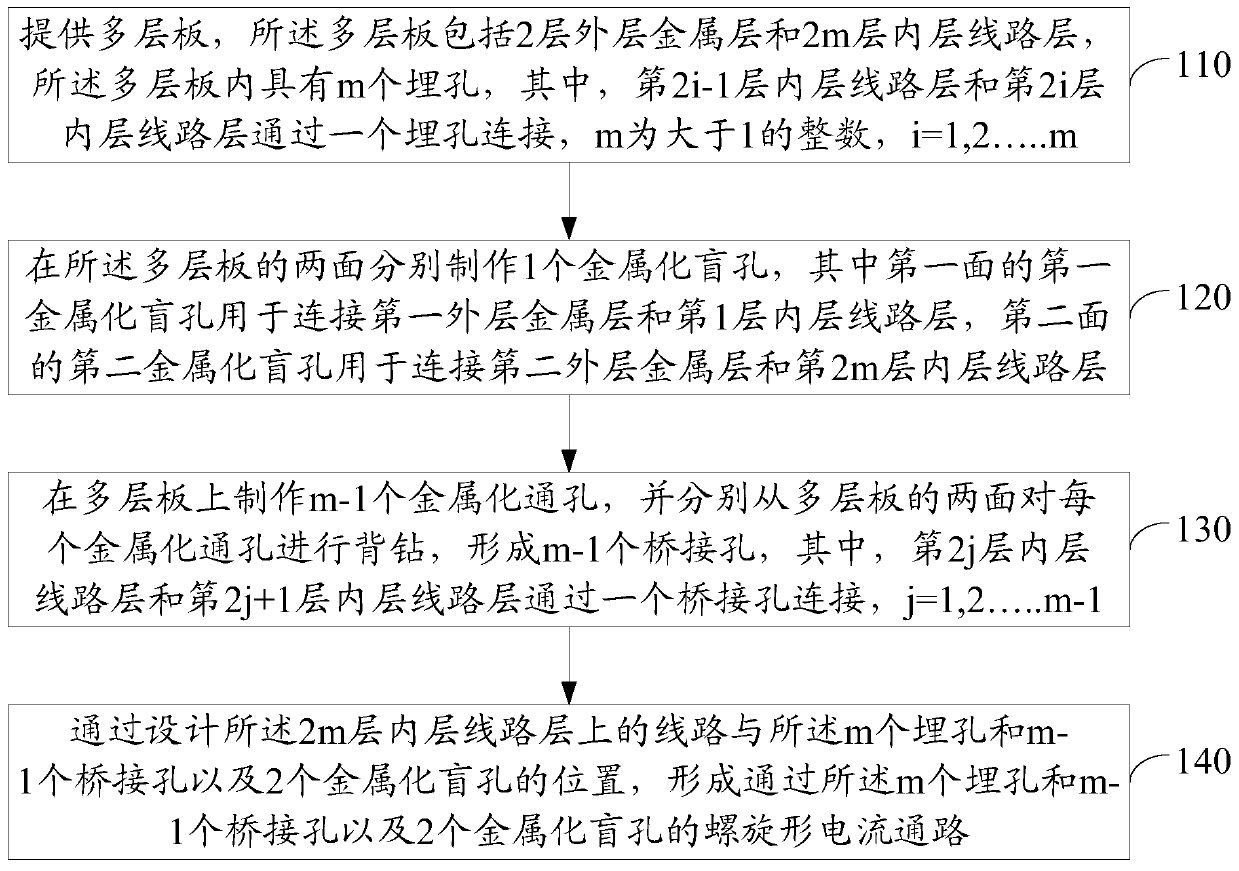
[0024] Please refer to figure 1 , an embodiment of the present invention provides a method for processing a circuit board, which may include:
[0025] 110. A multilayer board is provided, the multilayer board includes 2 outer metal layers and 2m inner circuit layers, m buried holes are provided in the multilayer board, wherein the 2i-1th inner circuit layer It is connected with the inner circuit layer of layer 2i through a buried hole, m is an integer greater than 1, i=1, 2...m;
[0026] 120. Make one metallized blind hole on both sides of the multilayer board, wherein the first metallized blind hole on the first side is used to connect the first outer metal layer and the first inner layer circuit layer, and the second The second metallized blind hole on the surface is used to connect the second outer metal layer and the 2mth inner layer circuit layer;
[0027] 130. Make m-1 metallized through holes on the multilayer board, and back-drill each metallized through hole from bo...
Embodiment 2
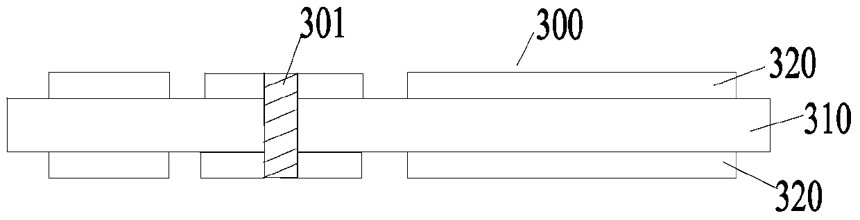
[0057] Please refer to Figure 3d , the embodiment of the present invention provides a multilayer circuit board, which may include:
[0058] 2 outer circuit layers, 2m inner circuit layers and m+1 insulating dielectric layers, where m is an integer greater than 1; wherein, the 2i-1th inner circuit layer and the 2ith inner circuit layer pass through a Buried hole connection, i=1,2.....m; the 2jth layer inner layer circuit layer and the 2j+1 layer inner layer circuit layer are connected through a bridge hole, j=1,2.....m-1; the 2nd layer An outer circuit layer and the first inner layer circuit layer are connected through the first metallized blind hole, and the second outer layer circuit layer and the 2mth inner layer circuit layer are connected through the second metallized blind hole; the multilayer circuit A spiral current path is formed in the board through the buried hole and the bridging hole as well as the first metallized blind hole and the second metallized blind hole....
PUM
 Abstract
Description
Claims
Application Information