Packaging structure and packaging method of multilayer chip

A packaging structure, multi-layer chip technology, applied in electrical components, electrical solid devices, circuits, etc., can solve the problems of inability to realize the electrical measurement of each layer of chips, inconvenient rework, etc., to reduce manufacturing costs, improve product yield, and simplify The effect of the operation steps

Inactive Publication Date: 2020-05-08
NAT CENT FOR ADVANCED PACKAGING
View PDF5 Cites 4 Cited by
  • Summary
  • Abstract
  • Description
  • Claims
  • Application Information

AI Technical Summary

Problems solved by technology

[0005] The technical problem to be solved by the present invention is: when the existing multi-layer chips are packaged, the electrical measurement of each layer of chips cannot be realized, and the problem of rework is not convenient; Packaging structure and packaging method for multi-layer chips that can effectively improve the yield rate of finished products

Method used


Image

  • Packaging structure and packaging method of multilayer chip
  • Packaging structure and packaging method of multilayer chip
  • Packaging structure and packaging method of multilayer chip

Examples


Embodiment 1

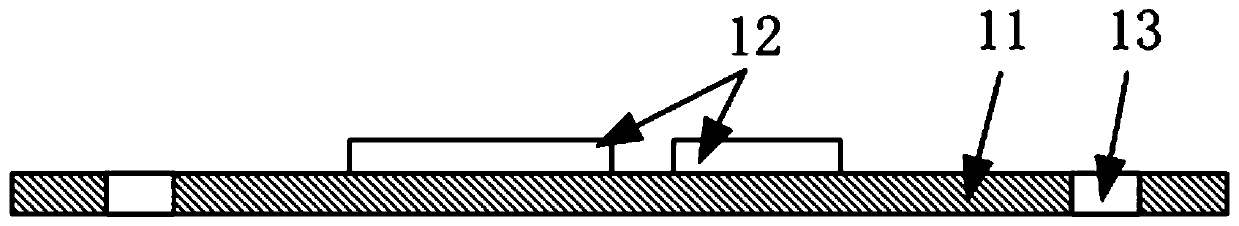
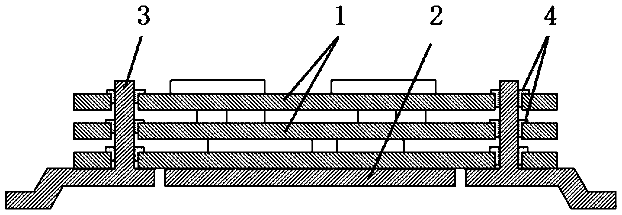
[0039] A packaging structure for multi-layer chips, such as figure 1 and figure 2 As shown, it includes a metal frame 2 , several column connectors 3 and several chip components 1 . Wherein, a number of chip components 1 are stacked sequentially above the metal frame 2 from top to bottom, and the bottom ends of the columnar connectors 3 are fixed on the upper surface of the metal frame 2 . Each chip assembly 1 includes a substrate 11, a chip unit 12 connected to the substrate 11, and a plurality of through holes 13 arranged on the substrate 11, such as figure 1 shown. In the present invention, the number of columnar connectors 3 is greater than or equal to the type of signal output of the chip component 1 in the packaging structure, and the position corresponding to each columnar connector 3 on the substrate 11 is provided with a through hole 13 for the penetration of the columnar connector 3 , Each columnar connector 3 can be connected to a chip component 1 with the same ...

Embodiment 2

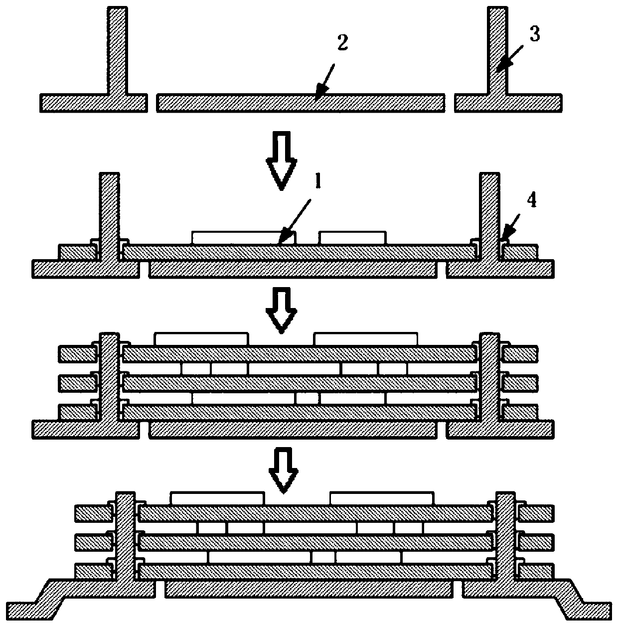
[0043] This embodiment provides a packaging method for a packaging structure of a multilayer chip, such as image 3 As shown, the specific process is as follows:

[0044] Step 1, preparing the metal frame 2 and several chip components 1 .

[0045] When the metal frame 2 is prepared, first fix the columnar connector 3 on the upper surface of the metal frame 2 according to the number of signal types output by a number of chip components 1 that need to be integrated, such as: a number of chip components 1 output When there are two signal types, no less than two columnar connectors 3 are set on the upper surface of the metal frame 2. In this embodiment, two columnar connectors 3 are set as an example, as image 3 shown;

[0046] When several chip components 1 are prepared, the preparation method of each chip component 1 is the same, and the chip monomer 12 is connected on the substrate 11, and a plurality of through holes 13 are arranged on the substrate 11 to obtain the chip co...


PUM


Abstract

The invention discloses a packaging structure and a packaging method of a multilayer chip. The packaging structure comprises a plurality of chip assemblies and a metal frame, wherein the chip assemblies and the metal frame are sequentially arranged in a stacked mode from top to bottom; each chip assembly comprises a substrate, a chip monomer connected to the substrate and a plurality of through holes formed in the substrate; a plurality of columnar connecting bodies are fixed on the upper surface of the metal frame; and the plurality of chip assemblies are all located above the metal frame, the through holes of the chip assemblies sleeve the columnar connecting body, and the substrates of the chip assemblies are communicated with the columnar connecting body through the welding body. According to the invention, the functions of fixing and communicating the columnar connecting body and the substrate are realized by adopting the welding body, the finished product yield of the integratedpackaging structure can be effectively improved, rework operation can be carried out on connection at the welding body position, and the preparation cost is reduced.

Description

technical field [0001] The invention relates to the packaging field, in particular to a packaging structure and packaging method for a multilayer chip. Background technique [0002] With people's continuous pursuit of miniaturization, systematization, and multi-function of electronic products, the feature size of VLSI is constantly shrinking. However, when the feature size of IC is about to reach the physical limit, people have to seek new technologies, new designs, and new materials to "beyond Moore". The system-in-package technology represented by 2.5D and 3D is a milestone on the road of "More than Moore". Among them, 2.5D packaging refers to the interconnection technology of stacked silicon chips, and 3D packaging uses through-silicon via technology to replace the traditional chip interconnection method with vertical short lines. [0003] In conventional 3D packaging, metal pillars are usually filled in through-silicon vias. For example, in the Chinese document CN1020...

Claims


Application Information

Patent Timeline
Patent Type & Authority Applications(China)
IPC IPC(8): H01L25/065H01L21/98H01L23/13H01L23/14H01L23/488
CPCH01L23/13H01L23/14H01L23/488H01L25/0652H01L25/50
Inventor 任玉龙孙鹏曹立强
Owner NAT CENT FOR ADVANCED PACKAGING
Why Eureka
Try Eureka