Eureka AIR delivers breakthrough ideas for toughest innovation challenges, trusted by R&D personnel around the world.

Delamination failure detection method of printed circuit board

A printed circuit board and detection method technology, applied in the direction of measuring devices, analyzing materials, and using wave/particle radiation for material analysis, etc., can solve problems such as improving the placement process, PCB delamination and blistering, economic losses, etc., and achieve convenience Mounting process, convenience and improved effect

Active Publication Date: 2018-12-04
GUANGZHOU FASTPRINT CIRCUIT TECH +2
View PDF4 Cites 0 Cited by
  • Summary
  • Abstract
  • Description
  • Claims
  • Application Information

AI Technical Summary

Problems solved by technology

[0003] During the placement process under lead-free conditions, PCBs often have the problem of delamination and blistering and failure, resulting in economic losses
Since there is no effective detection method for the cause of delamination failure, PCBs after delamination failure are often discarded without finding out the cause to improve the placement process

Method used


Image

  • Delamination failure detection method of printed circuit board

Examples


Embodiment Construction

[0027] Below in conjunction with accompanying drawing and specific embodiment, the present invention will be further described:

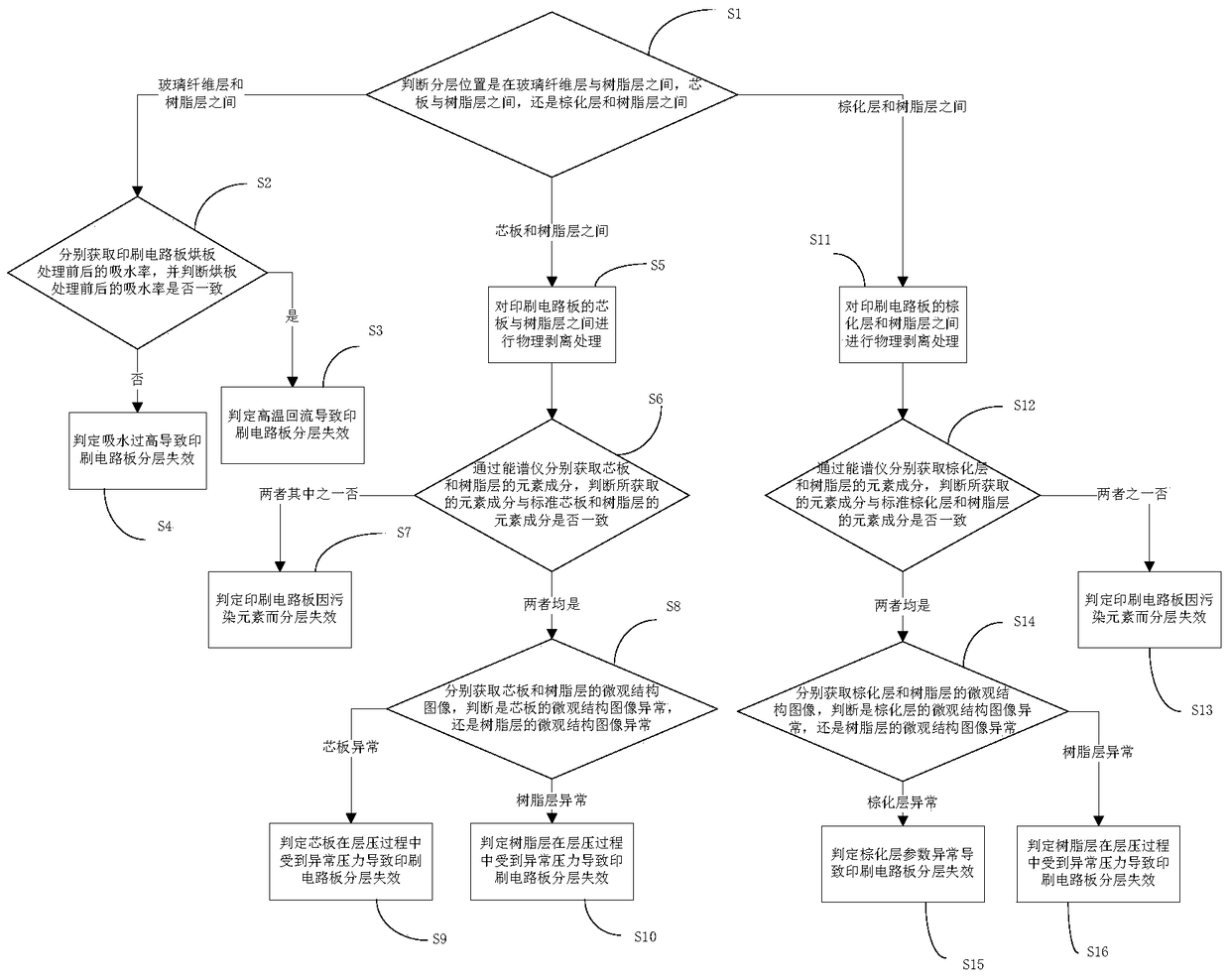
[0028] See figure 1 , the present invention relates to a kind of printed circuit board delamination failure detection method, and its preferred embodiment comprises the following steps:

[0029] Step S1: Vertically slice the delaminated printed circuit board to determine whether the delamination position is between the glass fiber layer and the resin layer, between the core board and the resin layer, or between the browning layer and the resin layer, if so Between the glass fiber layer and the resin layer, perform step S2; if it is between the core board and the resin layer, perform step S5; if it is between the browning layer and the resin layer, perform step S11;

[0030] Step S2: Obtain the water absorption rate of the printed circuit board before and after the drying plate treatment, and judge whether the water absorption rate before and after ...


PUM


Abstract

The invention relates to a printed circuit board layering failure detection method, which comprises the following steps that a layering fracture printed circuit board is subjected to vertical slicing so as to judge whether the layering position is between a glass fiber layer and a resin layer or between a core plate and the resin layer or between a browning layer and the resin layer; if the layering position is between the glass fiber layer and the resin layer, the layering failure reason is judged according to the water absorption rate before and after the board baking treatment of the printed circuit board; if the layering position is between the core plate and the resin layer, the layering failure reason is judged according to the element ingredients and the microstructure image of the core plate and the resin layer; if the layering position is between the browning layer and the resin layer, the layering failure reason is judged according to the element ingredients and the microstructure image of the browning layer and the resin layer. The method provided by the invention can be used for detecting the layering reason by aiming at different layering positions of the printed circuit board, so that the subsequent pasting process can be improved.

Description

technical field [0001] The invention relates to a method for detecting delamination failure of a printed circuit board. Background technique [0002] In order to meet the requirements of lead-free environmental protection, the PCB mounting process is also required to be carried out under lead-free conditions. The peak temperature of lead-free reflow is 235-255°C, which is 10-20°C higher than the previous leaded reflow, and the time at high temperature becomes longer. Therefore, the requirements for heat resistance of the PCB during the reflow process are higher. [0003] During the placement process under lead-free conditions, PCBs often have problems of delamination and blistering and failure, resulting in economic losses. Since there is no effective detection method for the cause of delamination failure, PCBs after delamination failure are often discarded without finding out the cause to improve the placement process. Contents of the invention [0004] Aiming at the d...

Claims


Application Information

Patent Timeline
Patent Type & Authority Patents(China)
IPC IPC(8): G01N23/00G01N23/22G01N5/00
CPCG01N5/00G01N23/00G01N23/22
Inventor 况东来胡梦梅陈蓓
Owner GUANGZHOU FASTPRINT CIRCUIT TECH
Why Eureka
Eureka Blog
Learn More