Check patentability & draft patents in minutes with Patsnap Eureka AI!

Thin film transistor array substrate

A technology of thin film transistors and array substrates, which is applied in the field of liquid crystal displays, can solve problems such as image retention, image flicker, and numerical values ​​that cannot be accurately measured, and achieve the effect of correcting the public voltage

Active Publication Date: 2016-06-01
WUHAN CHINA STAR OPTOELECTRONICS TECH CO LTD
View PDF4 Cites 6 Cited by
  • Summary
  • Abstract
  • Description
  • Claims
  • Application Information

AI Technical Summary

Problems solved by technology

However, by externally modifying the common voltage Vcom, due to the formula Among them, the value of some capacitors cannot be accurately measured, resulting in the inability to accurately correct the common voltage Vcom; and, with the long-term use of the liquid crystal display, the aging of the device and changes in the use environment (such as temperature, humidity, etc.) will also cause the feed-through voltage ΔV changes, if the common voltage Vcom cannot be corrected in time at this time, there will still be problems of image flicker or image retention, which will affect the display quality

Method used


Image

  • Thin film transistor array substrate
  • Thin film transistor array substrate
  • Thin film transistor array substrate

Examples


Embodiment 1

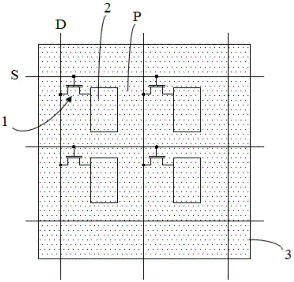
[0040] This embodiment provides a thin film transistor array substrate, such as Figure 4 As shown, the thin film transistor array substrate includes a plurality of scanning lines S and a plurality of data lines D, the plurality of scanning lines S and the plurality of data lines D perpendicularly intersect each other to define M rows×N columns of pixel units P, each pixel unit P includes at least a first thin film transistor 10 and a pixel electrode 20 , the gate of the thin film transistor 10 is electrically connected to the scan line S, the drain is electrically connected to the data line D, and the source is electrically connected to the pixel electrode 20 .

[0041] Further, the thin film transistor array substrate further includes a common electrode layer 30, wherein the common electrode layer 30 is divided into alternately spaced M first common electrodes 31 and M second common electrodes 32 along the row direction. The m first common electrode 31 and the m second commo...

Embodiment 2

[0051] The thin film transistor array substrate provided in this embodiment is different from Embodiment 1 in that in this embodiment, two second thin film transistors 40 are connected between the m first common electrode 31 and the m second common electrode 32 .

[0052] One of the preferred embodiments, such as Figure 9 As shown, the two second thin film transistors 40 are respectively arranged in the pixel unit P in the first column of the mth row and the Nth column of the mth row; the gates of the two second thin film transistors 40 are respectively connected to the first The drains of the scan lines S corresponding to the m rows of pixel units are respectively connected to the m th second common electrodes 32 , and the sources are respectively connected to the m th first common electrodes 31 .

[0053] In another preferred embodiment, as Figure 10 As shown, the two second thin film transistors 40 are arranged outside the pixel unit P in the mth row, and are respective...

Embodiment 3

[0056] The thin film transistor array substrate provided in this embodiment is different from Embodiment 1 in that the first common electrodes 31 and the second common electrodes 32 in this embodiment extend along the column direction.

[0057] Specifically, such as Figure 11 As shown, the thin film transistor array substrate includes a plurality of scanning lines S and a plurality of data lines D, the plurality of scanning lines S and the plurality of data lines D perpendicularly intersect each other to define M rows×N columns of pixel units P, each pixel unit P includes at least a first thin film transistor 10 and a pixel electrode 20 , the gate of the thin film transistor 10 is electrically connected to the scan line S, the drain is electrically connected to the data line D, and the source is electrically connected to the pixel electrode 20 .

[0058] Further, the thin film transistor array substrate further includes a common electrode layer 30, wherein the common electrod...


PUM


Abstract

The invention discloses a thin film transistor array substrate. The thin film transistor array substrate comprises M line*N column pixel units defined by multiple scan lines and multiple data lines in a mutual crossed manner; each pixel unit is provided with a first thin film transistor and a pixel electrode; the array substrate also comprises a common electrode layer; the common electrode layer is divided into multiple first common electrodes and multiple second common electrodes that are spaced alternately in a one-to-one correspondence manner along a line direction or a column direction; common voltage is input to each second common electrode; the common voltage is supplied to the corresponding first common electrode through at least one second thin film transistor; voltage drop [delta]V is generated when each data line charges the corresponding pixel electrode through the corresponding first thin film transistor; voltage drop [delta]Vcom is generated when each second common electrode charges the corresponding first common electrode through the corresponding second thin film transistor; the parameter of the second thin film transistor is configured to that the [delta]Vcom is equal to or close to the [delta]V, wherein M and N are integers greater than 1.

Description

technical field [0001] The invention relates to the technical field of liquid crystal displays, in particular to a thin film transistor array substrate. Background technique [0002] Liquid crystal display (Liquid Crystal Display, LCD) is a flat and ultra-thin display device, which consists of a certain number of color or black and white pixels, and is placed in front of a light source or a reflective surface. Liquid crystal displays have low power consumption, high image quality, small size, and light weight, so they are favored by everyone and become the mainstream of displays. Currently, the liquid crystal display is mainly a thin film transistor (Thin Film Transistor, TFT) liquid crystal display, and the liquid crystal panel is a main component of the liquid crystal display. [0003] A liquid crystal panel usually consists of a thin film transistor array substrate, a color filter substrate and a liquid crystal layer. Wherein, a plurality of pixel units (Pixel) are arra...

Claims


Application Information

Patent Timeline
Patent Type & Authority Applications(China)
IPC IPC(8): H01L27/12
CPCH01L27/124
Inventor 唐岳军李得俊崔宏青
Owner WUHAN CHINA STAR OPTOELECTRONICS TECH CO LTD
Features
  • R&D
  • Intellectual Property
  • Life Sciences
  • Materials
  • Tech Scout
  • Unparalleled Data Quality
  • Higher Quality Content
  • 60% Fewer Hallucinations
Learn More