Display panel, display device and manufacturing method of display panel

A display panel and plane technology, applied in semiconductor/solid-state device manufacturing, semiconductor devices, electrical components, etc., can solve problems such as high price, difficult bending, and discount of bendability of flexible display devices, and achieve performance improvement and bending resistance Strong folding effect

Active Publication Date: 2017-01-04
SHANGHAI TIANMA MICRO ELECTRONICS CO LTD +1
View PDF4 Cites 7 Cited by
  • Summary
  • Abstract
  • Description
  • Claims
  • Application Information

AI Technical Summary

Problems solved by technology

[0006] The film material of the protective film layer used today is generally polyethylene terephthalate (PET) base material, which is solid. In order to consider the problem of matching with the adhesive material and cost issues, such as image 3 As shown, the total thickness B' of the protective film layer 5' and the adhesive material 4' is generally set thicker, which cannot meet the requirement of a total thickness of 20um. The difficulty of the large lamination

Method used


Image

  • Display panel, display device and manufacturing method of display panel
  • Display panel, display device and manufacturing method of display panel
  • Display panel, display device and manufacturing method of display panel

Examples


Embodiment Construction

[0053] Example embodiments will now be described more fully with reference to the accompanying drawings. Example embodiments may, however, be embodied in many forms and should not be construed as limited to the embodiments set forth herein; rather, these embodiments are provided so that this disclosure will be thorough and complete, and will fully convey the concept of example embodiments to those skilled in the art. The same reference numerals denote the same or similar structures in the drawings, and thus their repeated descriptions will be omitted.

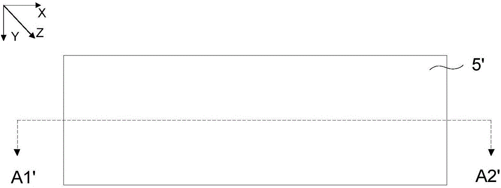
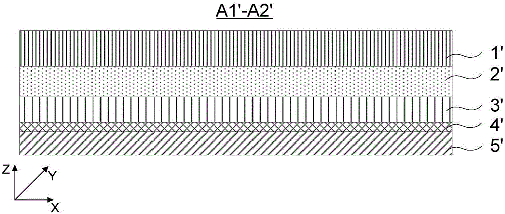
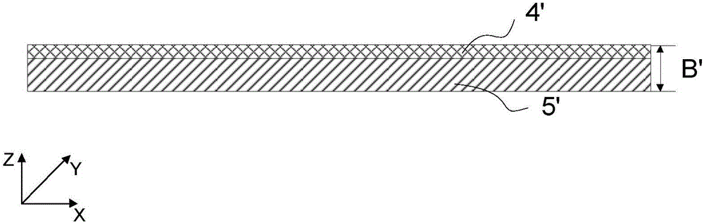
[0054] like Figure 4 As shown, it is a schematic top view of the protective layer of the display panel according to an embodiment of the present invention. like Figure 5 shown, for Figure 4 The cross-sectional view of the A1-A2 direction in the middle. An embodiment of the present invention provides a display panel, comprising Figure 5The protective film layer 5 , the flexible substrate 3 , the light emitting device 2...


PUM

PropertyMeasurementUnit
Thicknessaaaaaaaaaa
Wavelengthaaaaaaaaaa

Abstract

The invention provides a display panel, a display device and a manufacturing method of the display panel. The display panel comprises a flexible substrate, a light-emitting device and a protective film layer, wherein the light-emitting device is positioned on one side of the flexible substrate; the protective film layer is positioned on the side, deviating from the light-emitting device, of the flexible substrate; the protective film layer is in direct contact with the flexible substrate; a plurality of bulges are arranged on the side, deviating from the flexible substrate, of the protective film layer. The invention provides a technical scheme that a lower protective film in the prior art is substituted, and the protective film layer is directly formed on the flexible substrate and is in direct contact with the flexible substrate, so that the display panel is thinned while the flexible substrate is protected from scratches; the plurality of bulges are arranged on one side of the protective film layer, so that the bending resistance of the display panel is stronger; on the other hand, the protective film layer adopts a single-layer structure directly formed on the flexible substrate in a printing manner, so that an adhesive material is omitted, the problem of matching between a film material and the adhesive material is not involved, and the restorability of the display panel after the display panel is bent is improved.

Description

technical field [0001] The invention relates to the field of display technology, in particular to a display panel, a display device and a manufacturing method of the display panel that enhance the bending resistance of the display panel. Background technique [0002] A flexible display device is a deformable and bendable device made of soft materials. Flexible display devices in the prior art generally adopt OLED (Organic Light-Emitting Diode, Organic Light-Emitting Diode) technology. This technology has the advantages of low power consumption, small size, light weight, and various display methods, so it is widely used in various electronic product. [0003] like figure 1 Shown is a schematic top view of the protective film layer of the display panel in the flexible display device, as shown in figure 2 for figure 1 A cross-sectional view in the direction A1'-A2', wherein the display panel includes a flexible substrate 3', a light emitting device 2' and an encapsulation ...

Claims


Application Information

Patent Timeline
IPC IPC(8): H01L27/32H01L51/00H01L51/56
CPCH10K59/12H10K77/111H10K71/00Y02E10/549
Inventor 刘聪慧于泉鹏蔡雨李喜烈
Owner SHANGHAI TIANMA MICRO ELECTRONICS CO LTD
Why Eureka
Try Eureka