Manufacturing method of semiconductor device

A manufacturing method and semiconductor technology, applied in semiconductor/solid-state device manufacturing, electrical components, circuits, etc., can solve problems such as reducing the yield rate of semiconductor devices and affecting the performance of semiconductor devices, so as to prevent undercutting, improve performance, and avoid corrosion Effect

Active Publication Date: 2020-04-07
SEMICON MFG INT (SHANGHAI) CORP +1
View PDF4 Cites 0 Cited by
  • Summary
  • Abstract
  • Description
  • Claims
  • Application Information

AI Technical Summary

Problems solved by technology

The formation of the undercut easily affects the performance of the semiconductor device and reduces the yield of the semiconductor device

Method used


Image

  • Manufacturing method of semiconductor device
  • Manufacturing method of semiconductor device
  • Manufacturing method of semiconductor device

Examples


Embodiment Construction

[0039] In order to make the content of the present invention clearer and easier to understand, the content of the present invention will be further described below in conjunction with the accompanying drawings. Of course, the present invention is not limited to this specific embodiment, and general replacements known to those skilled in the art are also covered within the protection scope of the present invention.

[0040] Secondly, the present invention is described in detail by means of schematic diagrams. When describing the examples of the present invention in detail, for the convenience of illustration, the schematic diagrams are not partially enlarged according to the general scale, which should not be used as a limitation of the present invention.

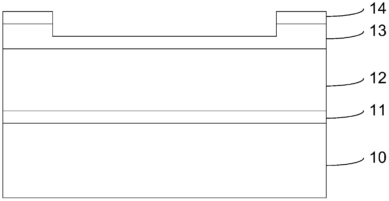
[0041] The structural diagram of each step of the manufacturing method of the semiconductor device well known to the inventor is as follows Figure 1~6 shown.

[0042] like figure 1 As shown, first a semiconductor substrat...


PUM


Abstract

The invention provides a semiconductor device manufacturing method, and the method comprises the steps: sequentially forming a low-k dielectric layer and a carbon-containing silicide layer on a semiconductor substrate; carrying out the plasma bombardment of the carbon-containing silicide layer, and enabling a part of carbon-containing silicide layer in the thickness direction to be converted intoa first barrier layer; forming a first groove in the first barrier layer and the carbon-containing silicide layer, carrying out the plasma bombardment of the surface of the first groove, and enablinga part of carbon-containing silicide layer in the width direction of the side wall of the first groove to be converted into a second barrier layer, wherein the second barrier layer completely covers the low-k dielectric layer. Because the etching rates of the etching liquid for the first barrier layer, the second barrier layer and the low-k dielectric layer are nearly equal in the forming processof a second groove, the method prevents chemical solution from corroding the surface of the low-k dielectric layer, thereby preventing the undercutting phenomenon, and improving the performances of asemiconductor device.

Description

technical field [0001] The invention relates to the technical field of semiconductors, in particular to a method for manufacturing a semiconductor device. Background technique [0002] With the development of semiconductor technology, integrated circuits are developing in the direction of high integration. The requirement of high integration makes the line width of semiconductor devices smaller and smaller, and the reduction of line width puts forward higher requirements for the manufacturing process of integrated circuits. [0003] Semiconductor devices are usually formed by multi-layer metal layers and multi-layer dielectric layers. The multi-layer metal layers are electrically connected by plugs arranged in the dielectric layers. As the line width decreases, the dielectric layer is now Dielectric materials with a low dielectric constant of less than 3 are often used. [0004] In the prior art, after forming a low-k (dielectric constant less than 3) dielectric layer, a h...

Claims


Application Information

Patent Timeline
Patent Type & Authority Patents(China)
IPC IPC(8): H01L21/768
Inventor 周鸣
Owner SEMICON MFG INT (SHANGHAI) CORP
Why Eureka
Try Eureka