Method for fabricating a CMOS image sensor

A technology of image sensor and manufacturing method, which is applied in semiconductor/solid-state device manufacturing, electric solid-state device, semiconductor device and other directions, and can solve the problems of complex manufacturing process, CCD cannot be applied to small products, complex driving mode, etc.

Inactive Publication Date: 2010-02-17
DONGBU HITEK CO LTD
View PDF7 Cites 0 Cited by
  • Summary
  • Abstract
  • Description
  • Claims
  • Application Information

AI Technical Summary

Problems solved by technology

[0004] However, this kind of CCD has various disadvantages such as complicated drive mode, high power consumption, etc.
In addition, the CDD usually requires a multi-step photolithography process, which makes the manufacturing process of the CCD relatively complicated
[0005] In addition, because it is difficult to integrate the controller, signal processor, and analog / digital converter (A / D converter) on a single chip of the CCD, the CCD may not be suitable for small products

Method used


Image

  • Method for fabricating a CMOS image sensor
  • Method for fabricating a CMOS image sensor
  • Method for fabricating a CMOS image sensor

Examples


Embodiment Construction

[0018] Hereinafter, a method of manufacturing a CMOS image sensor according to an embodiment of the present invention will be described in detail with reference to the accompanying drawings. Figure 2 to Figure 7 is a cross-sectional view schematically illustrating a method of manufacturing a CMOS image sensor according to various embodiments.

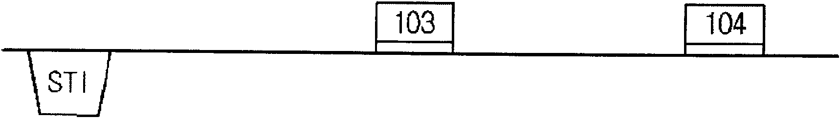
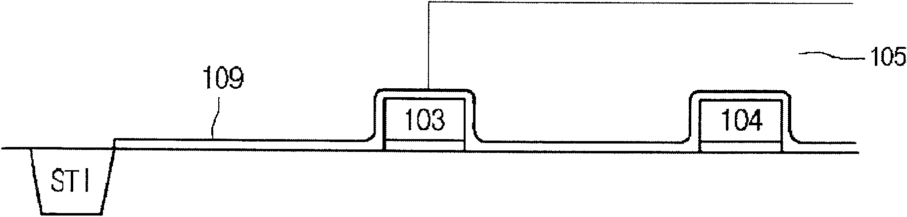
[0019] Such as figure 2 As shown, an active region and an isolation region are defined in a semiconductor substrate, and an isolation layer is formed in the isolation region by a shallow trench isolation (STI) process. Thereafter, a gate oxide is grown in the active region, and a conductive layer (such as a high-concentration polysilicon layer) is deposited on the semiconductor substrate. Then, part of the conductive layer and the gate oxide are selectively removed by a photolithography-etching process, thereby forming first and second gates 103 and 104 separated by a certain distance in the active region of the semiconductor substra...


PUM


Abstract

A method for fabricating a CMOS image sensor may include forming an isolation layer defining an active area on a semiconductor substrate, forming first and second gate electrodes in the transistor area of the semiconductor substrate, forming a photodiode area in the semiconductor substrate at a first side of the first gate electrode, forming an oxide layer over the photodiode area, the oxide layerhaving a thickness greater than that of the dielectric layer, forming a source / drain extension area in the semiconductor substrate at a second side of the second gate electrode and between the firstand second gate electrodes, forming source / drain regions in the transistor area of the semiconductor substrate by ion implantation through the dielectric layer, and forming a complementary ion implantation region in the photodiode area through the oxide layer.

Description

technical field [0001] The present invention relates to a method for manufacturing a CMOS image sensor. Background technique [0002] Image sensors are semiconductor devices for converting light images into electrical signals, and are mainly classified into Charge Coupled Devices (CCD) and Complementary Metal Oxide Semiconductor (CMOS) image sensors. [0003] The CCD has a plurality of photodiodes (PDs) arranged in a matrix to convert optical signals into electrical signals. The CCD includes: a plurality of vertical charge-coupled devices (VCCDs), arranged between a plurality of photodiodes vertically arranged in a matrix, so that charges are transmitted in a vertical direction when charges are generated from each photodiode; a plurality of horizontal charge-coupled devices ( HCCD) for horizontally transferring charges that have been transferred from the VCCD; and a sense amplifier for outputting charges by sensing the horizontally transferred charges. [0004] However, su...

Claims


Application Information

Patent Timeline
Patent Type & Authority Patents(China)
IPC IPC(8): H01L21/822H01L27/146
CPCH01L27/14689H01L27/14609H01L27/146
Inventor 沈喜成
Owner DONGBU HITEK CO LTD
Why Eureka
Try Eureka