Semiconductor discrete device storage life characteristic detection method and system

A storage life and feature detection technology, which is applied in the field of storage life feature detection of semiconductor discrete devices, can solve the problems of no storage life assessment method, inability to accurately evaluate the storage life of electronic components, batch failure of electronic components, etc.

Active Publication Date: 2017-03-29
CHINA ELECTRONICS PROD RELIABILITY & ENVIRONMENTAL TESTING RES INST THE FIFTH ELECTRONICS RES INST OF MIITCEPREI LAB
View PDF6 Cites 4 Cited by
  • Summary
  • Abstract
  • Description
  • Claims
  • Application Information

AI Technical Summary

Problems solved by technology

[0003] The storage life of traditional electronic components is usually based on the initial specified life given by the engineering experience of the research and development factory. In addition, during the entire development and use of missile weapons and equipment in service, storage tests have not been systematically carried out. Therefore, Unable to verify the storage life requirements proposed by the user
However, during the long-term storage of missiles, ele

Method used


Image

  • Semiconductor discrete device storage life characteristic detection method and system
  • Semiconductor discrete device storage life characteristic detection method and system

Examples


Embodiment Construction

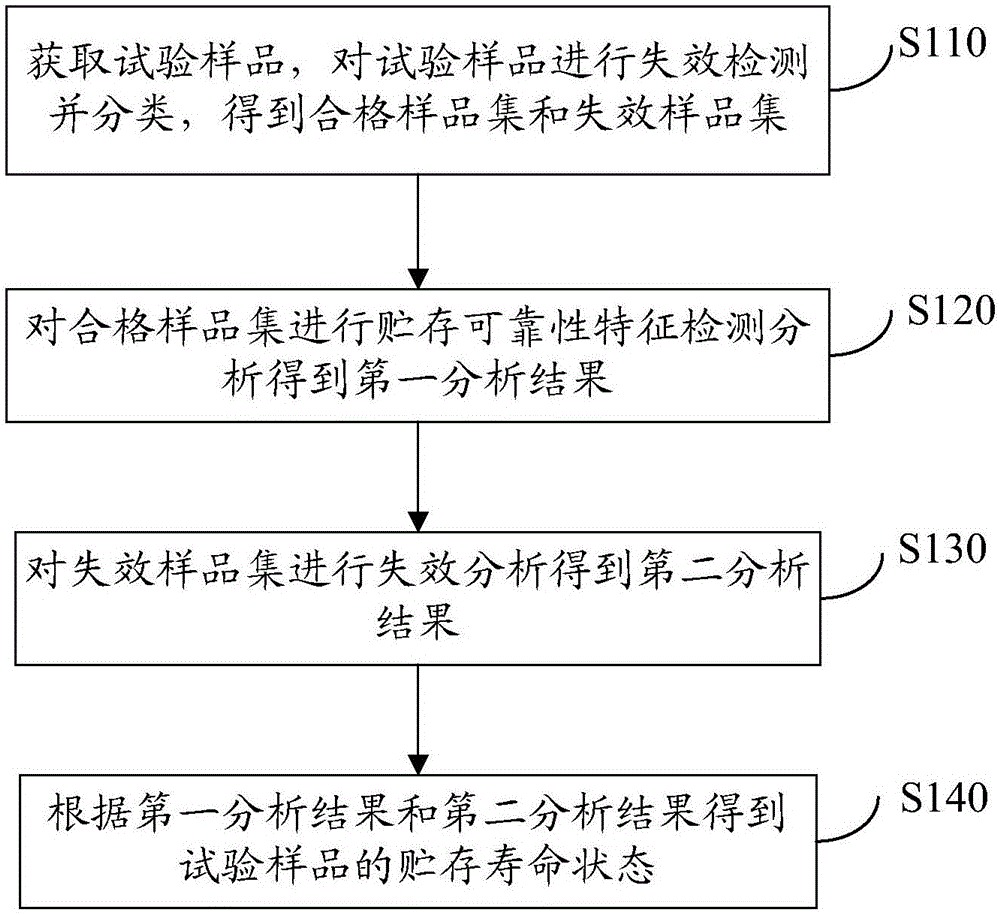
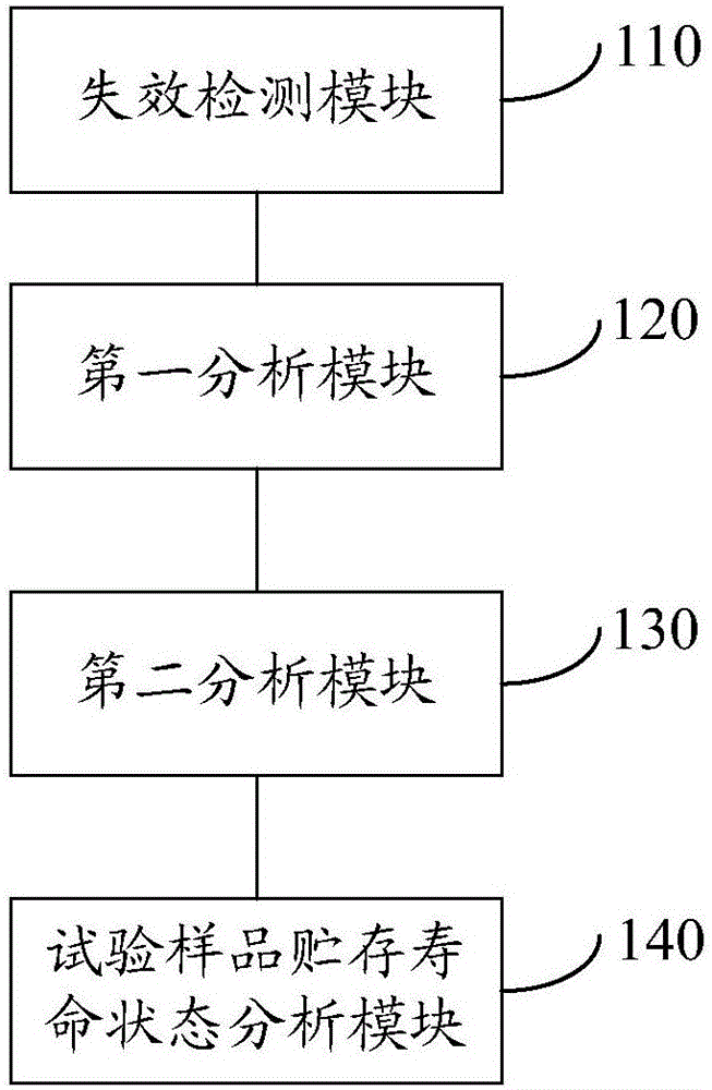
[0018] In one embodiment, a method for detecting storage life characteristics of semiconductor discrete devices, such as figure 1 shown, including the following steps:

[0019] Step S110: Obtain test samples, perform failure detection and classification on the test samples, and obtain a set of qualified samples and a set of failed samples.

[0020] Specifically, there is no unique method for failure detection of test samples, and conventional failure detection methods are applicable, specifically, appearance inspection, electrical parameter inspection, pressure test, etc.

[0021] In one embodiment, step S110 includes: measuring the electrical parameters of the test sample to determine whether the test sample has electrical failure; if not, classifying the corresponding test sample into a qualified sample set; if so, classifying the corresponding test sample into failure sample set.

[0022] Specifically, combined with the test sample device manual, set the test sample test ...


PUM


Abstract

The present invention relates to a semiconductor discrete device storage life characteristic detection method and system. The method includes the following steps that: test samples are obtained; failure detection and classification are performed on the test samples, so that a qualified sample set and a failure sample set can be obtained; storage reliability feature detection analysis is performed on the qualified sample set, so that a first analysis result can be obtained; failure analysis is performed on the failure sample set, so that a second analysis result is obtained; and the storage life states of the test samples can be obtained according to the first analysis result and the second analysis result. According to the semiconductor discrete device storage life characteristic detection method and system of the invention, the storage reliability feature detection analysis is performed on the qualified sample set, so that whether test samples having storage degradation failure characteristics exist in the qualified sample set can be judged; the failure analysis is performed on the failure sample set, so that whether test samples having storage failure information exist in the failure sample set can be judged; and the storage life states of the test samples can be obtained according to the analysis results. With the above scientific storage life evaluation method adopted, the storage life states of the test samples can be evaluated accurately and accurately.

Description

technical field [0001] The invention relates to the field of component detection, in particular to a method and system for detecting storage life characteristics of semiconductor discrete devices. Background technique [0002] As the basic components of weapons and equipment, electronic components have many varieties and are used in huge quantities. Semiconductor discrete devices are typical components, and the research on their storage life is of great significance. During the service period of the whole machine, the change law of its storage reliability over time and whether the guaranteed life of storage meets the application requirements are the key concerns of equipment development and use units. [0003] The storage life of traditional electronic components is usually based on the initial specified life given by the engineering experience of the research and development factory. In addition, during the entire development and use of missile weapons and equipment in serv...

Claims


Application Information

Patent Timeline
IPC IPC(8): G01D21/02
CPCG01D21/02
Inventor 罗琴李坤兰姚珂黄创绵胡湘洪
Owner CHINA ELECTRONICS PROD RELIABILITY & ENVIRONMENTAL TESTING RES INST THE FIFTH ELECTRONICS RES INST OF MIITCEPREI LAB
Why Eureka
Try Eureka