OLED (organic light emitting diode) display panel, method for driving same and display device

A display panel and display area technology, applied to static indicators, instruments, semiconductor devices, etc., can solve the problem of uneven display

Active Publication Date: 2018-01-19
WUHAN TIANMA MICRO ELECTRONICS CO LTD
View PDF6 Cites 35 Cited by
  • Summary
  • Abstract
  • Description
  • Claims
  • Application Information

AI Technical Summary

Problems solved by technology

[0004] Embodiments of the present invention provide an OLED display panel, a driving method thereof, and a display device to solve the problem of uneven display in the prior art

Method used


Image

  • OLED (organic light emitting diode) display panel, method for driving same and display device
  • OLED (organic light emitting diode) display panel, method for driving same and display device
  • OLED (organic light emitting diode) display panel, method for driving same and display device

Examples


Embodiment Construction

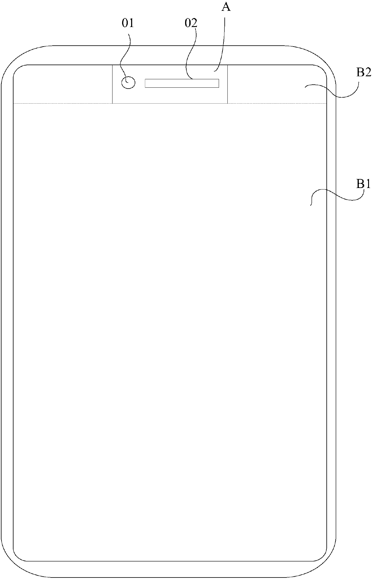
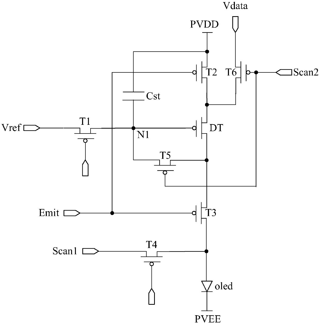
[0027] exist figure 1 In the display panel shown, since the number of pixels in a row of pixels in the first display area B1 is greater than the number of pixels in a row of pixels in the second display area B2, each row of pixels in the first display area B1 and the second display area B2 are connected The loads of the scanning signal lines are different. by figure 2 Take the pixel circuit shown as an example. When the load on the scan line is different, the signal delay time of the scan line Scan2 will be different, resulting in different charging speeds of Vdata to the N1 node, and different charging speeds of the N1 node will result in different potentials of the N1 node. Finally, because the N1 node potential of the pixel circuit in the first display area B1 is inconsistent with the N1 node potential of the pixel circuit in the second display area B2, the luminescent current generated by the pixel circuit in the first display area B1 is different from that in the second...


PUM


Abstract

The invention discloses an OLED (organic light emitting diode) display panel, a method for driving the same and a display device. The OLED display panel, the method and the display device have the advantages that high-level power voltages and low-level power voltages can be provided for various shift register units by a power supply; voltage difference values of the high-level power voltages and the low-level power voltages which are provided for the first register units by the power supply are first voltage difference, voltage difference values of the high-level power voltages and the low-level power voltages which are provided for the second register units by the power supply are second voltage difference, and the first voltage difference is unequal to the second voltage difference; thefirst voltage difference is unequal to the second voltage difference, accordingly, voltage amplitude of scanning signals received by pixel circuits in first display regions is unequal to voltage amplitude of scanning signals received by pixel circuits in second display regions, light emitting currents of the pixel circuits in the first display regions are consistent with light emitting currents ofthe pixel circuits in the second display regions under the condition of identical voltage data, and the problem of display unevenness can be solved.

Description

technical field [0001] The invention relates to the field of display technology, in particular to an OLED display panel, a driving method thereof and a display device. Background technique [0002] With the development of display technology, the full screen has a large screen-to-body ratio and an ultra-narrow bezel. Compared with ordinary display screens, it can greatly improve the visual effect of the viewer, and thus has received widespread attention. At present, in a display device with a full screen such as a mobile phone, in order to realize the functions of Selfie, video call and fingerprint recognition, a front camera, an earpiece, a fingerprint recognition area or physical buttons are usually arranged on the front of the display device. [0003] In an organic light emitting (Organic Light Emitting Diode, OLED) display device, in order to realize full-screen display, such as figure 1 As shown, the camera 01, earpiece 02 and other devices are generally arranged in the...

Claims


Application Information

Patent Timeline
Patent Type & Authority Applications(China)
IPC IPC(8): G09G3/3208
CPCG09G3/3233G09G3/3266G09G2300/0426G09G2300/0819G09G2300/0842G09G2300/0861G09G2310/0251G09G2310/0262G09G2310/0286G09G2330/028H10K59/121G09G3/3258G09G2310/0264H10K59/12
Inventor 李玥向东旭朱仁远高娅娜周星耀
Owner WUHAN TIANMA MICRO ELECTRONICS CO LTD
Why Eureka
Try Eureka