A microelectrode array chip and its manufacturing method
A technology of microelectrode array and manufacturing method, which is applied in the direction of circuits, electrical components, microstructure technology, etc., can solve problems such as the inability to accurately locate stimulation sites, achieve good insulation performance, light transmittance, and simple manufacturing process
- Summary
- Abstract
- Description
- Claims
- Application Information
AI Technical Summary
Problems solved by technology
Method used
Image


Examples
Embodiment 1
[0056] Such as Figure 1 to Figure 16 , the invention provides a kind of manufacturing method of microelectrode array chip, described manufacturing method comprises:
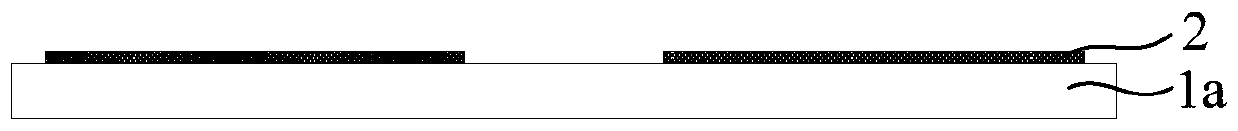
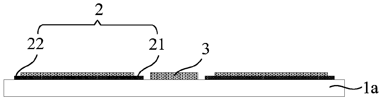
[0057] S1: providing a first substrate 1a, and forming a metal electrode array 2 on the first substrate 1a;
[0058] S2: forming an insulating layer 3 above the structure obtained in S1, etching the insulating layer 3 to expose the electrode site array 21 and electrode pins 22 on the metal electrode array 2, forming a micro-electrode array structure;
[0059] S3: providing a second substrate 1b, forming a micro-pipe pattern array 4 on the second substrate 1b;
[0060] S4: pouring a covering layer 5 over the structure formed in S3 to form grooves 8 corresponding to the micro-pipe pattern array 4 on the covering layer 5;
[0061] S5: Peel off the cover layer 5 and form a through hole through the groove 8 and the cover layer 5 at the outer edge of the groove 8 to form an inlet array 10;
[0062] S6: Align and bo...
Embodiment 2
[0104] Such as Figure 15 with Figure 16 As shown, the micro-electrode array chip of the present invention is produced through the above-mentioned manufacturing process, including: a micro-electrode array structure, a micro-pipeline array structure located above the micro-electrode array structure, and a micro-pipe array structure located above the micro-pipe array structure culture chamber ring; wherein,
[0105] The micropipe array structure is composed of a plurality of micropipes, and the micropipe includes a groove, a stimulation port and a sample inlet respectively connected to both ends of the groove, wherein the stimulation port is connected to the microelectrode array structure. The electrode sites are corresponding, and both the stimulation port and the electrode sites are located inside the culture chamber ring, and the sample inlet is located outside the culture chamber ring.
PUM
| Property | Measurement | Unit |
|---|---|---|
| thickness | aaaaa | aaaaa |
| diameter | aaaaa | aaaaa |
| diameter | aaaaa | aaaaa |
Abstract
Description
Claims
Application Information
 - R&D
- Intellectual Property
- Life Sciences
- Materials
- Tech Scout
- Unparalleled Data Quality
- Higher Quality Content
- 60% Fewer Hallucinations
Browse by: Latest US Patents, China's latest patents, Technical Efficacy Thesaurus, Application Domain, Technology Topic, Popular Technical Reports.
© 2025 PatSnap. All rights reserved.Legal|Privacy policy|Modern Slavery Act Transparency Statement|Sitemap|About US| Contact US: help@patsnap.com