
Organic light-emitting display panel, preparation method therefor, and organic light-emitting display device

A technology for light-emitting display and organic light-emitting devices, which is applied in semiconductor/solid-state device manufacturing, semiconductor devices, electrical components, etc., and can solve problems such as changes and color shift of OLED display devices

Active Publication Date: 2018-08-03
WUHAN TIANMA MICRO ELECTRONICS CO LTD
View PDF4 Cites 8 Cited by
  • Summary
  • Abstract
  • Description
  • Claims
  • Application Information

AI Technical Summary

Problems solved by technology

[0004] However, while improving the luminous efficiency and brightness of the OLED device, the microcavity effect often causes the electroluminescent spectrum of the OLED display device to change with the change of the observation angle, resulting in color shift when the OLED display device is observed at a large viewing angle.

Method used


Image

  • Organic light-emitting display panel, preparation method therefor, and organic light-emitting display device
  • Organic light-emitting display panel, preparation method therefor, and organic light-emitting display device
  • Organic light-emitting display panel, preparation method therefor, and organic light-emitting display device

Examples


preparation example Construction

[0054] This embodiment also provides a method for preparing an organic light-emitting display panel, such as figure 1 and Figure 9 as shown, Figure 9 It is a schematic flow chart of the method for preparing an organic light-emitting display panel provided in this embodiment; the preparation method includes:

[0055] S1: providing a base substrate 10;

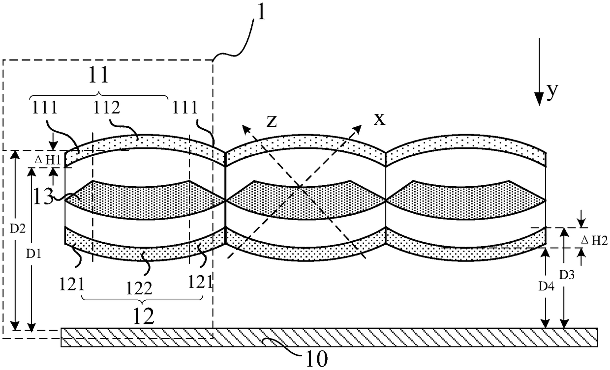
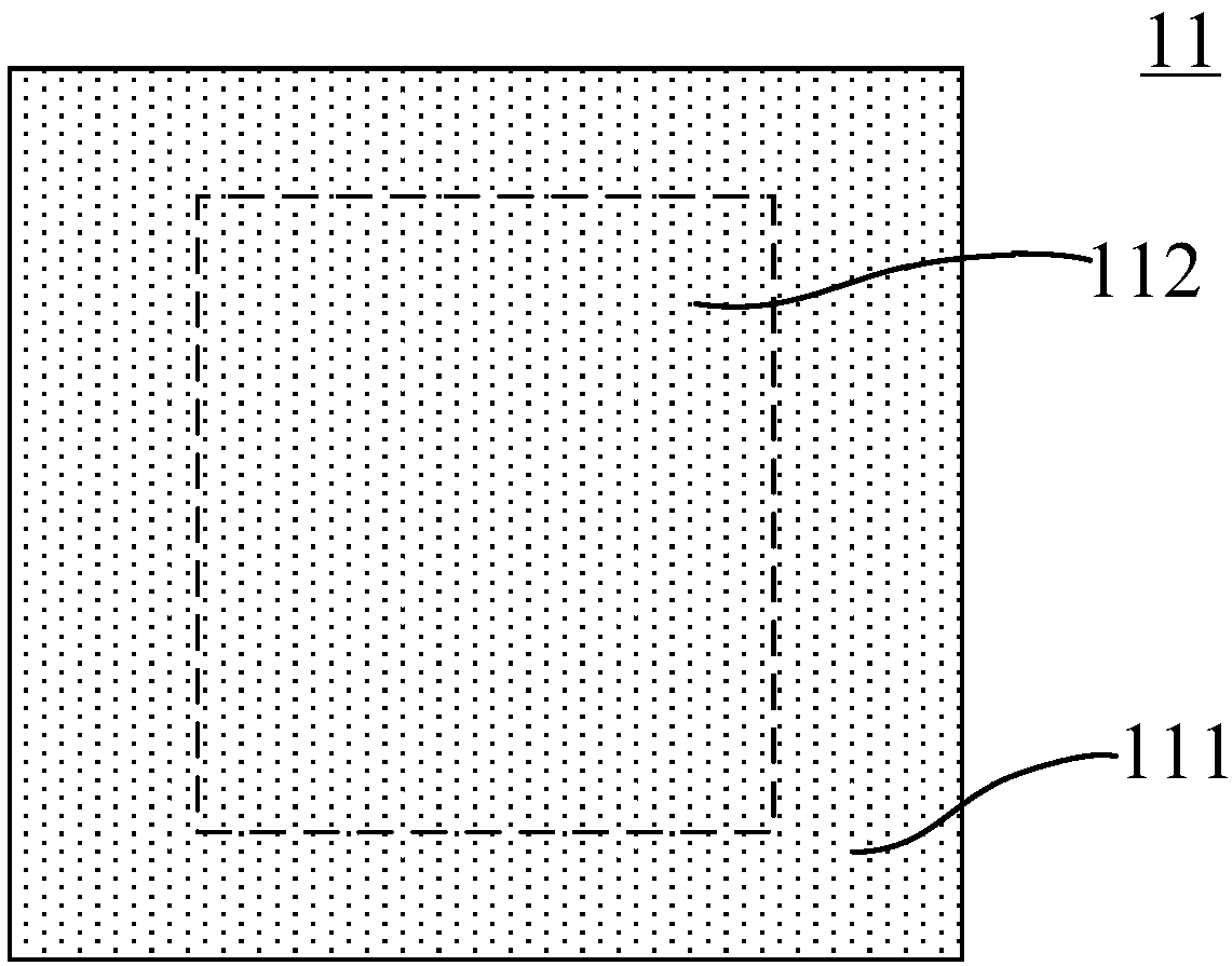
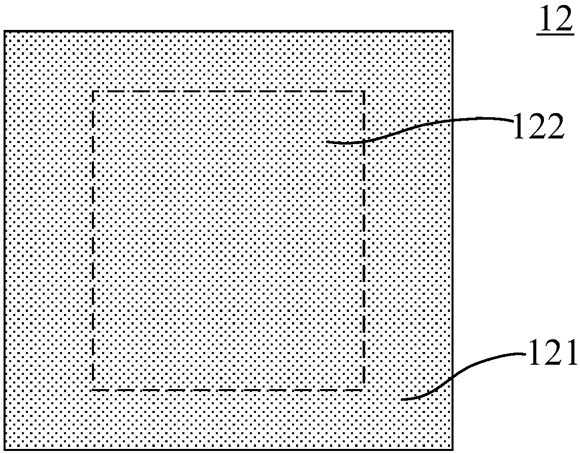
[0056] S2: Form a plurality of organic light-emitting devices 1 on one side of the base substrate 10; the organic light-emitting device 1 includes a first electrode 11, a light-emitting layer 13, and a second electrode 12 stacked along a first direction y; the first direction y is The direction perpendicular to the surface of the base substrate 10; the first electrode 11 includes a first edge electrode 111 and a first intermediate electrode 112 surrounded by the first edge electrode 111; the vertical distance between the first edge electrode 111 and the surface of the base substrate 10 D1, less than the vertical distance D2...


PUM


Abstract

The invention provides an organic light-emitting display panel and a display device thereof, relates to the technical field of display, and is used for improving the big-view-angle color cast of an organic light-emitting display panel. The organic light-emitting display panel comprises a plurality of organic light-emitting devices formed at one side of a substrate. Each organic light-emitting device comprises a first electrode, a light-emitting layer and a second electrode, wherein the first electrode, the light-emitting layer and the second electrode are stacked in a first direction, and thefirst direction is a direction perpendicular to the substrate. Each first electrode comprises a first edge electrode and a first central electrode surrounded by the first edge electrode. The verticaldistance between each first edge electrode and the substrate is less than the vertical distance between each first central electrode and the substrate. Each second electrode comprises a second edge electrode and a second central electrode surrounded by the second edge electrode, wherein the vertical distance between each second edge electrode and the substrate is less than the vertical distance between each second central electrode and the substrate. The organic light-emitting display panel is used for image display.

Description

technical field [0001] The present invention relates to the field of display technology, in particular to an organic light emitting display panel, a preparation method thereof, and an organic light emitting display device. Background technique [0002] Organic Light-Emitting Diode (hereinafter referred to as OLED) display panels are widely used in the field of display technology because of their many advantages such as active light emission, high contrast ratio, and no viewing angle limitation. In a traditional OLED display panel structure, in order to improve the luminous efficiency of the OLED device, a microcavity structure is usually used to enhance the luminescence of the OLED device. [0003] Since the microcavity can increase the emission rate at the resonant wavelength while suppressing the emission rate at the non-resonant wavelength, the microcavity structure can significantly narrow the emission spectrum, increase the peak value, and improve the brightness and lum...

Claims


Application Information

Patent Timeline
IPC IPC(8): H01L27/32H01L21/77
CPCH01L21/77H10K59/00
Inventor 程爽牛晶华王湘成朱晴杨闰
Owner WUHAN TIANMA MICRO ELECTRONICS CO LTD
Learn More