Unlock instant, AI-driven research and patent intelligence for your innovation.

Data output buffer

一种输出缓冲器、数据的技术,应用在缓冲器领域,能够解决微凸块难以区分、微凸块焊盘尺寸小、半导体器件生产率降低等问题

Active Publication Date: 2018-08-21
SK HYNIX INC
View PDF8 Cites 7 Cited by
  • Summary
  • Abstract
  • Description
  • Claims
  • Application Information

AI Technical Summary

Problems solved by technology

[0006] However, the size of the microbump pads is very small, making it difficult for microbumps to distinguish defective (or failed) portions caused by damage to actual package balls from those caused by misalignment between the socket and package balls of test equipment. defect part
Therefore, although the actual package balls are not damaged during the test of the semiconductor device, the occurrence of defective parts is shielded, resulting in a decrease in the productivity of the semiconductor device

Method used


Image

  • Data output buffer
  • Data output buffer
  • Data output buffer

Examples


Embodiment Construction

[0014] Reference will now be made to embodiments of the present disclosure, examples of which are illustrated in the accompanying drawings. Wherever possible, the same reference numbers will be used throughout the drawings to refer to the same or like parts.

[0015] For reference, embodiments including additional components may be provided. Furthermore, depending on the embodiment, an active high or active low configuration indicating the activation state of a signal or circuit may be changed. Also, the configuration of a logic gate or logic gates required to realize the same function or operation may be modified. That is, a configuration of logic gates for one type of operation and another configuration of logic gates for the same type of operation can be substituted for each other depending on the specific situation. Various logic gates can be applied to implement these configurations, if desired.

[0016] Various embodiments of the present disclosure may be directed to ...


PUM


Abstract

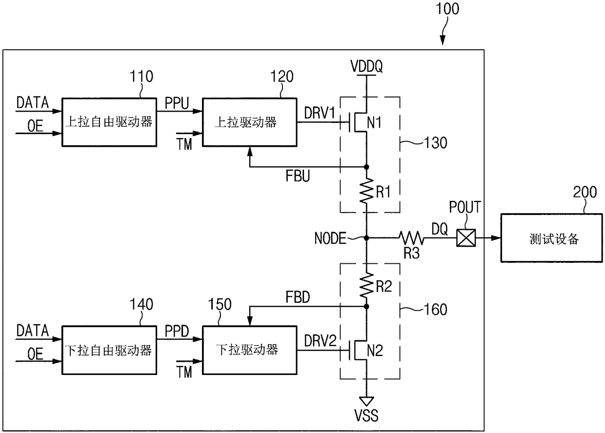
A data output buffer may be provided. The data output buffer may include a pull-up circuit configured to output a pull-up feedback signal by pull-up driving an output node. The data output buffer mayinclude a pull-up driver configured to output the pull-up drive signal by driving a pull-up signal, and selectively activate the pull-up drive signal based on the pull-up feedback signal. The data output buffer may include a pull-down circuit configured to output a pull-down feedback signal by pull-down driving the output node based on a pull-down drive signal. The data output buffer may include apull-down driver configured to output the pull-down drive signal by driving a pull-down signal, and selectively activate the pull-down drive signal based on the pull-down feedback signal.

Description

[0001] Cross References to Related Applications [0002] This application claims priority based on Korean Patent Application No. 10-2017-0019266 filed on February 13, 2017, the entire contents of which are hereby incorporated by reference. technical field [0003] Embodiments of the present invention may relate generally to a buffer, and more particularly to a data output buffer. Background technique [0004] Various semiconductor devices (eg, CPUs, memories, gate arrays, etc.) implemented as integrated circuit (IC) chips are incorporated into various electronic products such as personal computers (PCs), servers, workstations, and the like. In general, a semiconductor device includes a reception circuit configured to receive various signals from the outside through input pads and an output circuit configured to transmit internal signals to the outside via output pads. [0005] A device for outputting one or more signals to the outside via a semiconductor device is called a ...

Claims


Application Information

Patent Timeline
Patent Type & Authority Applications(China)
IPC IPC(8): G11C7/10
CPCG11C7/1057G11C29/1201G11C29/08G11C29/12
Inventor 黄美显
Owner SK HYNIX INC
Features
  • R&D
  • Intellectual Property
  • Life Sciences
  • Materials
  • Tech Scout
  • Unparalleled Data Quality
  • Higher Quality Content
  • 60% Fewer Hallucinations
Learn More