Display panel, manufacturing method of display panel and display device

A technology for display panels and manufacturing methods, applied in semiconductor/solid-state device manufacturing, organic semiconductor devices, semiconductor devices, etc., capable of solving problems such as short circuits, affecting the display effect of organic electroluminescent devices, leakage, etc.

Active Publication Date: 2018-11-27
BOE TECH GRP CO LTD
View PDF6 Cites 13 Cited by
  • Summary
  • Abstract
  • Description
  • Claims
  • Application Information

AI Technical Summary

Problems solved by technology

[0002] In existing organic electroluminescent devices, the pixel defining layer generally has a roughly trapezoidal shape, and the width of the upper part is smaller than that of the lower part

Method used


Image

  • Display panel, manufacturing method of display panel and display device
  • Display panel, manufacturing method of display panel and display device
  • Display panel, manufacturing method of display panel and display device

Examples


Embodiment Construction

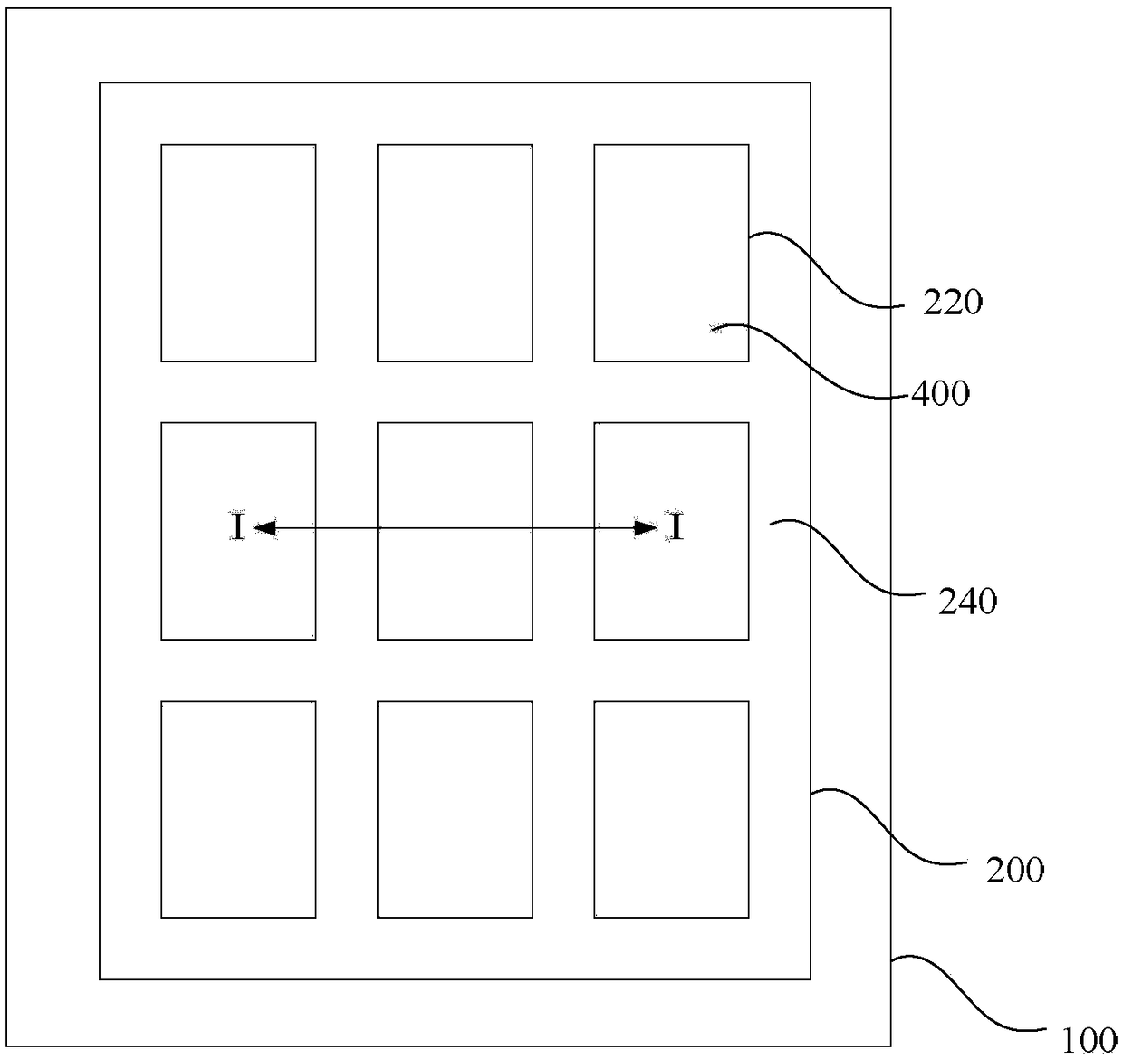
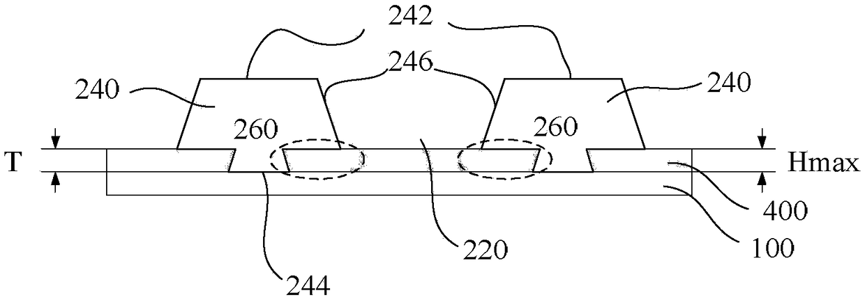
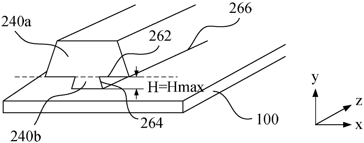
[0026] In order to make the purpose, technical solutions and advantages of the embodiments of the present disclosure clearer, the technical solutions of the embodiments of the present disclosure will be clearly and completely described below in conjunction with the accompanying drawings of the embodiments of the present disclosure. Apparently, the described embodiments are some of the embodiments of the present disclosure, not all of them. Based on the described embodiments of the present disclosure, all other embodiments obtained by persons of ordinary skill in the art without creative effort fall within the protection scope of the present disclosure.

[0027] Unless otherwise defined, the technical terms or scientific terms used herein shall have the usual meanings understood by those having ordinary skill in the art to which the present disclosure belongs. "First", "second" and similar words used in the specification and claims of the present disclosure do not indicate any ...


PUM


Abstract

The invention discloses a display panel, a manufacturing method of the display panel and a display device. The display panel comprises a base plate, a pixel defining layer and a first electrode, wherein the pixel defining layer is positioned on the base plate and comprises a plurality of openings and separation levees; each separation levee is surrounded at each opening and comprises a top surface, a bottom surface and at least one side surface; the side surface connects the top surface and the bottom surface; the area of the top surface is greater than the area of the bottom surface; the at least one side surface comprises a notch; the first electrode is positioned at the bottom of each opening and extends to the notch; relative to the base plate, the height of the first electrode is smaller than or equal to the maximum height of the notch. The height of the first electrode is smaller or equal to the maximum height of the notch relative to the surface of the base plate, so that the first electrode cannot climb to the upper part of the separation levee; the electric leakage risk is reduced.

Description

technical field [0001] Embodiments of the present disclosure relate to the field of display technology, and in particular, to a display panel, a manufacturing method thereof, and a display device. Background technique [0002] In existing organic electroluminescent devices, the pixel defining layer generally has a roughly trapezoidal shape, and the width of the upper part is smaller than that of the lower part. The wall and the upper part will cause a short circuit between the anode and the cathode, or cause the risk of leakage, thereby affecting the display effect of the organic electroluminescent device. Contents of the invention [0003] Embodiments of the present disclosure provide a display panel and a manufacturing method thereof, which can at least solve at least one of the above problems. [0004] The first aspect of the present disclosure provides a display panel. The display panel comprises: a substrate; a pixel defining layer located on the substrate, the pixe...

Claims


Application Information

Patent Timeline
IPC IPC(8): H01L27/32H01L51/52H01L51/56
CPCH10K59/122H10K50/81H10K59/1201H10K71/00H10K2102/341H10K59/121
Inventor 侯文军
Owner BOE TECH GRP CO LTD
Why Eureka
Try Eureka