Printed-circuit board preparation method capable of avoiding galvanic effect
A printed circuit board and Giavani effect technology, applied in the field of printed circuit board preparation, can solve the problems of insufficient fluidity of the adhesive, poor product effect, cumbersome operation and other problems, so as to avoid Giavani effect. Effect, easy removal, high precision effect
- Summary
- Abstract
- Description
- Claims
- Application Information
AI Technical Summary
Problems solved by technology
Method used
Image

Examples
Embodiment Construction
[0031] In order to enable those skilled in the art to better understand the technical solutions of the present invention, the technical solutions in the embodiments of the present invention will be clearly and completely described below in conjunction with the drawings in the embodiments of the present invention. Obviously, the described implementation Examples are only some of the embodiments of the present invention, not all of them. Based on the embodiments of the present invention, all other embodiments obtained by persons of ordinary skill in the art without making creative efforts shall fall within the protection scope of the present invention.
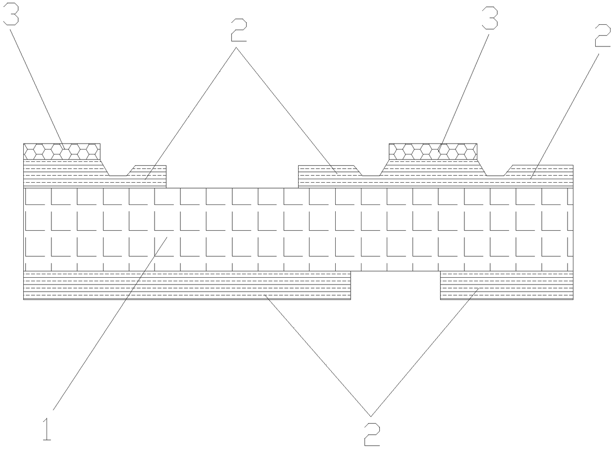
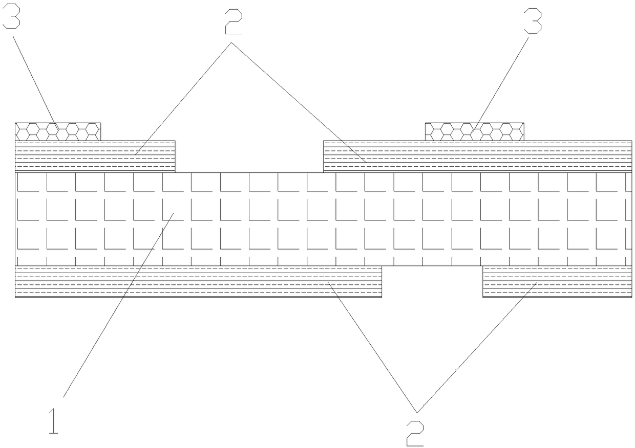
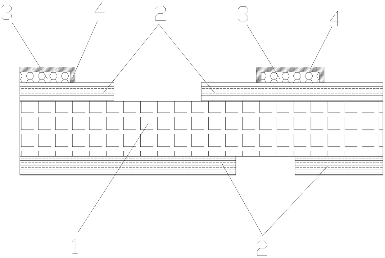
[0032] see Figure 2 to Figure 6 , a method for preparing a printed circuit board avoiding the Giavani effect of the present embodiment, specifically includes the following steps, such as Image 6 Shown:
[0033] Step S1: Prepare the substrate
[0034] The substrate includes a dielectric material 1 in the middle, a copper lay...
PUM
 Abstract
Description
Claims
Application Information