Fabrication method of lead-contained PCB at groove bottom of stepped groove and PCB

A manufacturing method and technology of stepped grooves, which are applied in multilayer circuit manufacturing, printed circuit manufacturing, conductive pattern layout details, etc., can solve the problems of copper open circuit, corrosion, slow oxidation of copper, etc., and achieve the effect of good electrical performance.

Active Publication Date: 2019-07-26
DONGGUAN SHENGYI ELECTRONICS
View PDF5 Cites 1 Cited by
  • Summary
  • Abstract
  • Description
  • Claims
  • Application Information

AI Technical Summary

Problems solved by technology

[0004] This method has the following disadvantages: due to the method of slotting first and then gold plating on the bottom of the slot, if the edges around the bottom of the stepped slot are bent, worn or damaged during use, the gold layer will be separated from the slot wall, causing If the copper layer on the side and bottom of the gold layer is exposed, the copper and gold will be exposed to the air at the same time, which will easily cause the Galvani effect (that is, the galvanic battery reaction), resulting in slow oxidation and corrosion of copper, resulting in a broken copper open circuit

Method used


Image

  • Fabrication method of lead-contained PCB at groove bottom of stepped groove and PCB
  • Fabrication method of lead-contained PCB at groove bottom of stepped groove and PCB
  • Fabrication method of lead-contained PCB at groove bottom of stepped groove and PCB

Examples


Embodiment Construction

[0035] In order to make the purpose, features and advantages of the present invention more obvious and understandable, the technical solutions in the embodiments of the present invention will be clearly and completely described below in conjunction with the accompanying drawings in the embodiments of the present invention. Obviously, the following The described embodiments are only some, not all, embodiments of the present invention. Based on the embodiments of the present invention, all other embodiments obtained by persons of ordinary skill in the art without making creative efforts belong to the protection scope of the present invention.

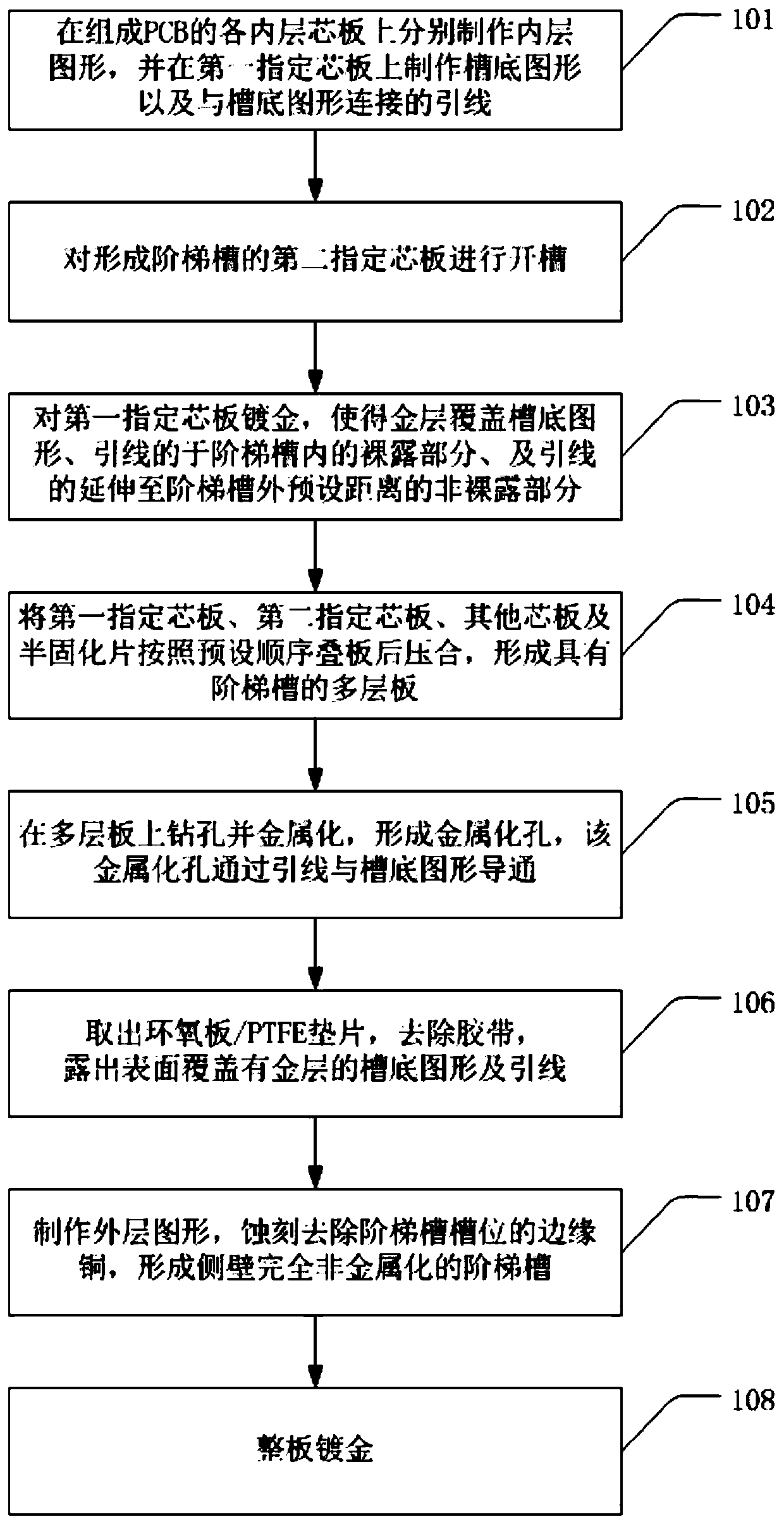
[0036] see figure 1 , the PCB fabrication method that the embodiment of the present invention provides comprises steps:

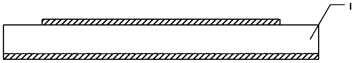
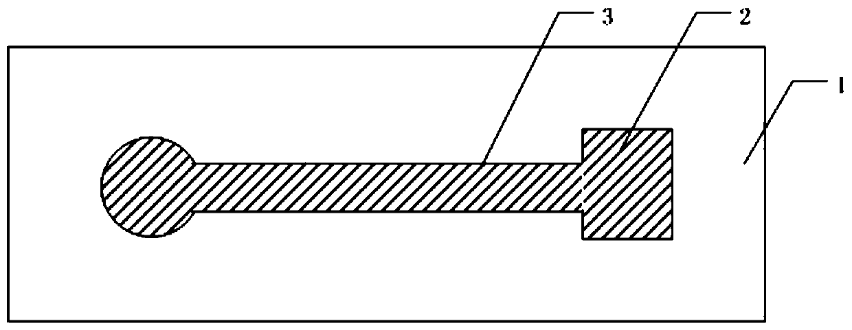
[0037] Step 101, making inner layer graphics on each inner layer core board forming the PCB, and making groove bottom graphics 2 and lead wires 3 connected to groove bottom graphics 2 on the first designated core boar...


PUM


Abstract

The invention relates to the technical field of PCBs, and discloses a fabrication method of a lead-contained PCB at the groove bottom of a stepped groove and the PCB. The PCB fabrication method comprises the steps of fabricating a groove bottom pattern and a lead on a first designated core board; grooving a second designated core board formed with the step groove; plating gold on the first designated core board so that a gold layer covers the groove bottom pattern, an exposed part, in the step groove, of the lead and an exposed part, extending to the step groove at a preset distance, of the lead; stacking and laminating the first designated core board, the second designated core board and other core boards forming the PCB according to a preset sequence to form a multi-layer board with thestep groove; and drilling and metalizing the multi-layer board to form a metal hole, wherein the metal hole is conducted with the groove bottom pattern by the lead. According to the fabrication methoddisclosed by the embodiment of the invention, the gold plating region is expanded by a mode of firstly plating the gold on the core boards and then forming the step groove, and copper and gold are prevented from being simultaneously exposed in air.

Description

technical field [0001] The invention relates to the technical field of PCB (Printed Circuit Board, printed circuit board), in particular to a method for manufacturing a PCB with lead wires at the bottom of a stepped groove and the PCB. Background technique [0002] With the upgrading of market demand, PCB is developing in the design direction of thinning, high density and three-dimensional structure on the premise of satisfying the good electrical and thermal performance of electronic products. PCB with stepped grooves has become an important development direction, and it has a wide range of applications in three-dimensional three-dimensional assembly, reducing the assembly volume of electrical equipment, and special electrical properties. [0003] For the PCB with non-metallization of the groove wall, making circuit patterns and leads at the bottom of the groove, and gold-plated PCB, the current ideal production method is to make circuit patterns at the bottom of the groove...

Claims


Application Information

Patent Timeline
Patent Type & Authority Applications(China)
IPC IPC(8): H05K3/46H05K1/02
CPCH05K1/0298H05K3/4611H05K3/4697
Inventor 何平刘梦茹袁继旺陈正清
Owner DONGGUAN SHENGYI ELECTRONICS
Why Eureka
Try Eureka