Unlock instant, AI-driven research and patent intelligence for your innovation.

Array substrate, display panel and display device

An array substrate and display area technology, applied in electrical components, electrical solid devices, circuits, etc., can solve problems such as affecting user experience, split screen, weak coupling capacitance, etc.

Active Publication Date: 2019-05-07
XIAMEN TIANMA MICRO ELECTRONICS
View PDF5 Cites 8 Cited by
  • Summary
  • Abstract
  • Description
  • Claims
  • Application Information

AI Technical Summary

Problems solved by technology

[0004] However, since the notch screen is equipped with special-shaped grooves, for the special-shaped display area, a gate line passes through fewer sub-pixels, so compared with the normal display area, the coupling capacitance of the M1 metal layer in the special-shaped display area is weaker. , so that the Gate delay (delay) phenomenon in the special-shaped display area is reduced, which in turn causes the brightness of the special-shaped display area to be higher, and the overall screen appears to display split screens, which affects the user experience.

Method used


Image

  • Array substrate, display panel and display device
  • Array substrate, display panel and display device
  • Array substrate, display panel and display device

Examples


Embodiment Construction

[0050] The full screen is currently the panel structure with the highest panel display ratio, so the display panel with full screen design is becoming more and more popular among consumers. A relatively common full screen adopts the "notch" design represented by the iPhone X. This kind of screen can also be called a notch screen. , three-dimensional recognition sensors and infrared sensors and other components.

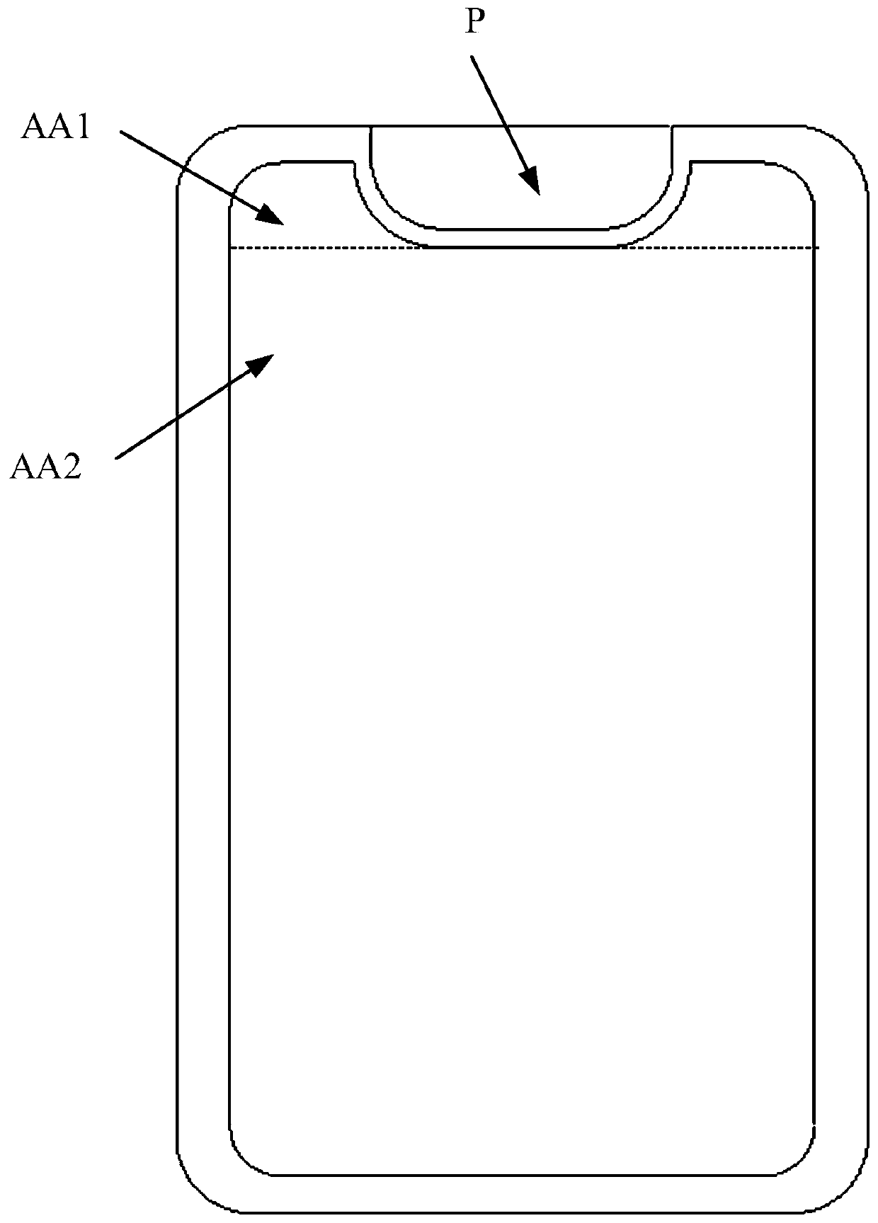
[0051] See Figure 1 ~ Figure 3 , figure 1 It is a top view schematic diagram of the notch screen in the prior art, figure 2 It is a schematic diagram of the panel wiring of the notch screen, image 3 for figure 2 An enlarged schematic view of part I of .

[0052] Such as figure 1As shown, the notch screen is generally provided with a special-shaped groove P at the top of the screen, so the display area of ​​the notch screen will be divided into two parts, that is, the bottom of the special-shaped groove P is used as the dividing line, and the display area is ...


PUM


Abstract

The invention discloses an array substrate, a display panel and a display device, which belongs to the technical field of display and is used for improving a phenomenon of split-screen display of a notch screen in the prior art. The first region of the array substrate includes a first display area, the second region includes a second display area located at the periphery of a first non-display area, and the number of any row of sub-pixels in the second display area is less than the number of any row of sub-pixels in the first display area. The array substrate further comprises a first metal layer, a second metal layer and an active layer, wherein the first metal layer and the second metal layer are arranged on an underlayer substrate, the active layer is located between the underlayer substrate and the first metal layer, the second metal layer includes a plurality of data lines, each data line is wired along a first direction of the underlayer substrate, and the first metal layer includes a plurality of grid lines intersected with the data lines; and the active layer located in the first non-display area is provided with a plurality of active structures, and each first active structure is overlapped with the grid lines located in the first non-display area in the direction perpendicular to the underlayer substrate.

Description

technical field [0001] The present invention relates to the field of display technology, in particular to an array substrate, a display panel and a display device. Background technique [0002] The full screen is currently the panel structure with the highest panel display ratio, so the display panel with full screen design is becoming more and more popular among consumers. A relatively common full screen adopts the "notch" design represented by the iPhone X. This kind of screen can also be called a notch screen. , three-dimensional recognition sensors and infrared sensors and other components. [0003] The existing special-shaped display area (Active Area, AA) near the full-screen notch can be driven by an interlace scanning (interlace) driving manner. Among them, the gate (gate) line runs straight through the special-shaped display area through the M1 metal layer, that is, only one gate line is used for each row, and the data (data) line crosses the gate line of the spec...

Claims


Application Information

Patent Timeline
IPC IPC(8): H01L27/12
Inventor 郑丽华李燕梅周璐陈国照
Owner XIAMEN TIANMA MICRO ELECTRONICS