A method for manufacturing a printed circuit board, a printed circuit board, and electronic equipment

A technology for printed circuit boards and manufacturing methods, which is applied in the directions of printed circuit manufacturing, printed circuits, electrical components, etc., can solve the problems of high-speed signals, difficulty in wiring, and wiring crossing the back-drilled level, etc., to reduce wiring interference, The effect of avoiding signal loss and reducing production difficulty

Active Publication Date: 2020-09-29
INSPUR BUSINESS MACHINE CO LTD
View PDF3 Cites 0 Cited by
  • Summary
  • Abstract
  • Description
  • Claims
  • Application Information

AI Technical Summary

Problems solved by technology

[0003] At present, the fan-out (Fanout) method is generally used when the BGA chip in the server PCB goes out. The signal is distorted
Therefore, in order to reduce signal loss, it is necessary to reduce the impact of via stubs through back-drilling. However, due to the back-drilling process, back-drilled holes are larger in diameter than ordinary vias, causing the back-drilled area to be used for wiring and The area of ​​copper laying is reduced. At the same time, the hole after back drilling needs to avoid the wiring and copper foil farther away, making it difficult to get out of the area where the BGA chip is located, resulting in chaotic wiring layout, and may also cause a large number of wiring to cross the back when going out. High-speed signal loss caused by drilling level

Method used


Image

  • A method for manufacturing a printed circuit board, a printed circuit board, and electronic equipment
  • A method for manufacturing a printed circuit board, a printed circuit board, and electronic equipment
  • A method for manufacturing a printed circuit board, a printed circuit board, and electronic equipment

Examples


Embodiment 1

[0052] Embodiment 1 of the present application provides a method for manufacturing a printed circuit board, which will be described in detail below with reference to the accompanying drawings.

[0053] see Figure 7 , which is a flowchart of a method for manufacturing a printed circuit board provided in Embodiment 1 of the present application.

[0054] The printed circuit board produced by this method includes a device layer and a multi-layer wiring layer, and a first preset number of solder ball array packaged BGA chips are arranged on the device layer. A BGA chip packaged in a solder ball array is taken as an example for illustration.

[0055] The method described in the embodiment of the present application includes the following steps:

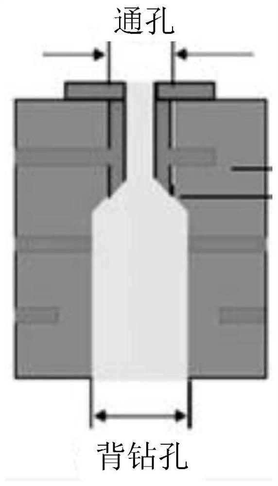
[0056] S701: Divide back-drilled holes required for routing into a second preset number of categories.

[0057] When wiring, classify the back-drilled holes required for wiring in advance, and classify the back-drilled holes that need t...

Embodiment 2

[0077] Based on the manufacturing method of the printed circuit board provided in the above-mentioned embodiments, Embodiment 2 of the present application also provides a printed circuit board. For the structure of the printed circuit board, please refer to Figure 8 shown.

[0078] The printed circuit board includes: a device layer and a multi-layer wiring layer, on which a solder ball array package BGA chip is arranged. The printed circuit board is manufactured using the method described in Embodiment 1, which will not be repeated here.

[0079] Utilizing the printed circuit board provided by the embodiment of the present application can avoid the signal loss caused by too many lines crossing the back-drilled hole level when the high-speed signal in the BGA chip goes out of the PCB, and can also arrange the line sequence and reduce the wiring level.

Embodiment 3

[0081] Based on the method for manufacturing a printed circuit board provided in the foregoing embodiments, Embodiment 3 of the present application further provides an electronic device, which will be described in detail below with reference to the accompanying drawings.

[0082] see Figure 12 , which is a schematic diagram of an electronic device provided in Embodiment 3 of the present application.

[0083] The electronic device 1200 includes a printed circuit board 1201 .

[0084] All or part of the printed circuit boards on the electronic device 1200 are fabricated using the method described in the first embodiment above.

[0085] The electronic device may be a communication or consumer electronic product such as a server or a notebook computer, which is not specifically limited in this application.

[0086] Since all or part of the printed circuit board on the electronic device is manufactured by the method described in the first embodiment above, it is possible to avoi...


PUM


Abstract

The application provides a method for fabricating a printed circuit board. The printed circuit board includes a device layer and a plurality of wiring layers, wherein the device layer is provided witha first predetermined number of ball grid array (BGA) chips. The method includes steps of dividing back drill holes required by wiring into a second predetermined number of categories; determining the total number of the wiring layers including the back drill holes according to the second predetermined number of categories; and using the device layer as a first layer, arranging wires layer by layer in an depth-to-shallow order according to the depth of the back drill holes, wherein the back drill holes of the wiring layer where the wires are arranged earlier are close to the BGA chips, and the back drill holes of the wiring layer where the wires are arranged later are away from the BGA chips. The method can avoid the signal loss caused by too many wires spanning the back drill hole layerswhen the high-speed signal in the BGA chips is out of the PCB, can also arrange the wire sequence, reduce the wiring layers, and reduce the difficulty of manufacturing the printed circuit board. Theapplication also provides a printed circuit board and an electronic device.

Description

technical field [0001] The present application relates to the technical field of hardware packaging, in particular to a method for manufacturing a printed circuit board, a printed circuit board and electronic equipment. Background technique [0002] As the functions of the current server become more and more powerful, the transmission rate of the internal signal of the server is increasing day by day, so the requirements for the performance of the high-speed signal transmission of the server are also getting higher and higher. However, since the chips packaged on the server PCB (Printed Circuit Board, printed circuit board) are becoming more and more dense, the signal performance of the BGA (Ball Grid Array, solder ball array package) chip wiring in the PCB has become a factor that affects the server's high-speed signal transmission performance. Key factor. [0003] At present, the fan-out (Fanout) method is generally used when the BGA chip in the server PCB goes out. The ...

Claims


Application Information

Patent Timeline
Patent Type & Authority Patents(China)
IPC IPC(8): H05K3/00
Inventor 曹颖男宋明哲
Owner INSPUR BUSINESS MACHINE CO LTD
Why Eureka
Try Eureka