
Potential measurement device

a technology of potential measurement and measuring device, which is applied in the direction of measuring device, instruments, scientific instruments, etc., can solve the problems of limiting the number of amplifiers, and increasing the number of simultaneous measurement points, so as to reduce the noise of wiring

Active Publication Date: 2018-12-06
SONY SEMICON SOLUTIONS CORP
View PDF4 Cites 0 Cited by
  • Summary
  • Abstract
  • Description
  • Claims
  • Application Information

AI Technical Summary

Benefits of technology

The present patent aims to reduce wiring noise and create a device that measures potential with low noise levels.

Problems solved by technology

However, the number of amplifiers is limited, and the number of simultaneous measurement points is also limited.
In the latter potential measurement device, the individual amplifiers are simultaneously operated, which leads to an increase in the number of simultaneous measurement points.
However, it is pointed out that, in the latter potential measurement device, there is a trade-off relationship between the number of simultaneous measurement points and noise, specifically, for example, the size of each amplifier is small, but noise is large (e.g., see Non-Patent Document 3).

Method used


Image

  • Potential measurement device
  • Potential measurement device
  • Potential measurement device

Examples


embodiment 1

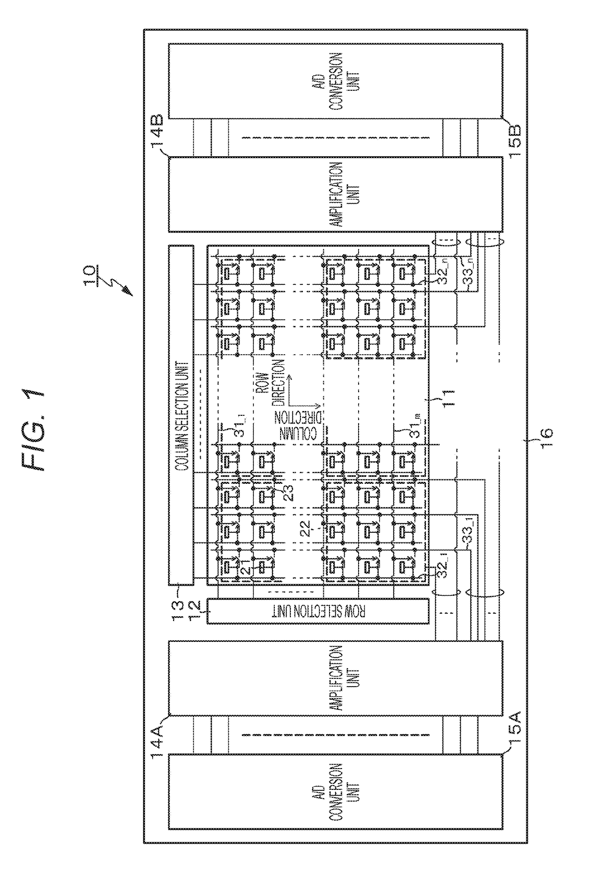
[0050]FIG. 1 is a configuration diagram schematically illustrating a configuration of a potential measurement device according to Embodiment 1. A potential measurement device 10 according to this embodiment has a configuration in which an electrode unit 11 which is created using a CMOS integrated circuit technique, a row selection unit 12, a column selection unit 13, amplification units 14A and 14B, and A / D conversion units 15A and 15B are integrated on one semiconductor substrate (semiconductor chip) 16. Herein, the configuration in which the amplification unit 14A and the A / D conversion unit 15A, and the amplification unit 14B and the A / D conversion unit 15B are respectively arranged at both sides with the electrode unit 11 interposed therebetween is employed. Alternatively, a configuration in which the amplification units and the A / D conversion units are arranged at one side of the electrode unit 11 may be employed.

[0051]In the electrode unit 11, m rows and n columns of a plurali...

embodiment 2

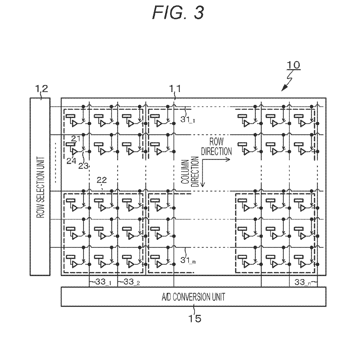
[0063]Embodiment 2 is a modified example of Embodiment 1. FIG. 3 schematically illustrates a configuration of a potential measurement device according to Embodiment 2. The potential measurement device 10 according to Embodiment 1 has a configuration in which a plurality of differential amplifiers 24 of the amplification units 14A and 14B is commonly provided for the plurality of read-out electrodes 21 arranged in an array shape. On the other hand, the potential measurement device 10 according to Embodiment 2 has a configuration in which the differential amplifiers 24 are respectively provided for the plurality of read-out electrodes 21 arranged in an array shape.

[0064]Further, in each of the plurality of read-out electrodes 21, the switches 23 are each provided between the output end of the corresponding differential amplifier 24 and the corresponding one of the signal read-out lines 33—1 to 33—n. Each switch 23 is driven to be turned on by the row selection signal applied from the ...

embodiment 3

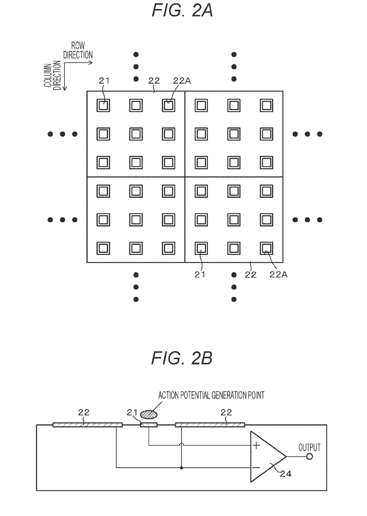
[0066]Embodiment 3 is a modified example of Embodiment 1. FIG. 4 illustrates a wiring structure between each of the read-out electrodes 21 and the reference electrode 22 and the differential amplifier 24 in a potential measurement device according to Embodiment 3. Embodiment 1 has a configuration in which the electrode size of each reference electrode 22 is set to be larger than the electrode size of each read-out electrode (see FIG. 2A). On the other hand, Embodiment 3 has a configuration in which the electrode size of each reference electrode 22 is set to be smaller than the electrode size of each read-out electrode 21.

[0067]Such an electrode layout example is suitable for cases where the size of a cell is approximately the same as the size of each read-out electrode, or the size of a cell is larger than the size of each read-out electrode. In such cases, electric charge uniformly reaches the entire area of each electrode, so that the amount of electric charge is in proportion to ...


PUM

PropertyMeasurementUnit
sizeaaaaaaaaaa
sizeaaaaaaaaaa
action potentialaaaaaaaaaa

Abstract

A potential measurement device according to the present disclosure includes a plurality of read-out electrodes arranged in an array shape and configured to detect a potential at a potential generation point generated due to a chemical change, and a reference electrode configured to detect a reference potential. The reference electrode is arranged within the array of the read-out electrodes. With this configuration, a low-noise potential measurement device in which noise superimposed on a wire from each of the read-out electrodes to an amplifier and noise superimposed on a wire from the reference electrode to the amplifier, i.e., wiring noise, can be reduced is achieved.

Description

TECHNICAL FIELD[0001]The present disclosure relates to a potential measurement device.BACKGROUND ART[0002]A potential measurement device has a configuration in which fine read-out electrodes are arranged in an array shape to electrochemically measure a potential generated due to a chemical change of a solution placed on the read-out electrodes. For example, there is a potential measurement device having a configuration in which living cells are placed on read-out electrodes filled with a culture solution, to thereby measure an action potential generated by living cells (e.g., see Patent Document 1). In particular, a potential measurement device having a configuration in which electrodes, amplifiers, A / D converters, and the like are integrated on one semiconductor substrate (chip) by using a complementary metal oxide semiconductor (CMOS) integrated circuit technique, to thereby measure potentials at multiple points at the same time has recently been attracting attention.[0003]Potenti...

Claims


Application Information

Patent Timeline
Patent Type & Authority Applications(United States)
IPC IPC(8): G01N27/416G01N27/30G01N27/403
CPCG01N27/416G01N27/301G01N27/403G01N27/30G01N27/27G01N33/48728G01N33/4836
Inventor OGI, JUNOIKE, YUSUKE
Owner SONY SEMICON SOLUTIONS CORP
Learn More