Pixel structure and display panel

A technology of pixel structure and pixel electrode, which is applied in the direction of instruments, semiconductor devices, optics, etc., and can solve the problems of affecting display effect and low pixel aperture ratio of liquid crystal display

Active Publication Date: 2021-01-08
HKC CORP LTD
View PDF14 Cites 0 Cited by
  • Summary
  • Abstract
  • Description
  • Claims
  • Application Information

AI Technical Summary

Problems solved by technology

However, liquid crystal displays have the problem of low pixel aperture ratio, which affects the display effect

Method used


Image

  • Pixel structure and display panel
  • Pixel structure and display panel
  • Pixel structure and display panel

Examples


Embodiment Construction

[0042] The following will clearly and completely describe the technical solutions in the embodiments of the application with reference to the drawings in the embodiments of the application. Apparently, the described embodiments are only some of the embodiments of the application, not all of them. Based on the embodiments in this application, all other embodiments obtained by persons of ordinary skill in the art without creative efforts fall within the protection scope of this application.

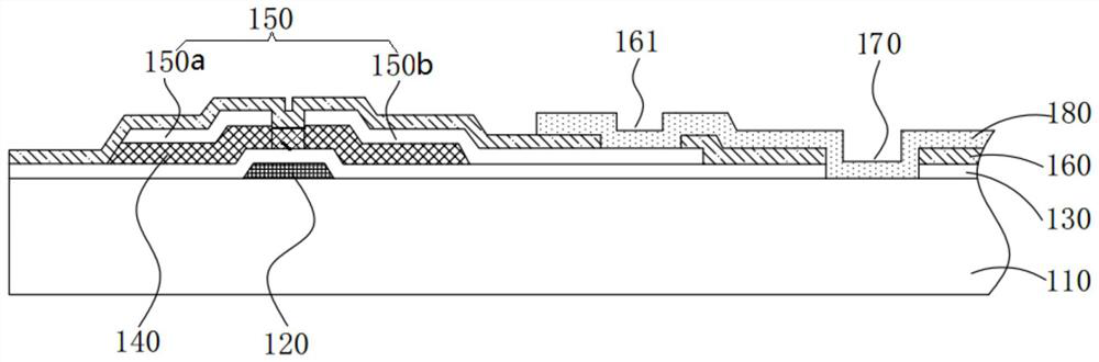
[0043] Such as figure 1 , figure 2 As shown, a pixel structure 100 provided in an embodiment of the present application. The pixel structure 100 includes a substrate 110 , an active switching element disposed on the substrate 110 , a pixel electrode 180 and a plurality of insulating layers 130 , 160 . Specifically, as figure 1 The active switching element of the pixel structure shown in includes a first metal layer 120, a second metal layer 150 and a semiconductor layer 140, wherein, wi...


PUM


Abstract

The embodiments of the present invention disclose a pixel structure and a display panel. The pixel structure comprises a substrate, an active switching element disposed on the substrate, a pixel electrode disposed on the substrate and electrically connected with the active switching element, and a plurality of insulating layers stacked between the pixel electrode and the substrate; the pixel structure further comprises a groove; the groove extends through the plurality of insulating layers; and the pixel electrode extends into the groove and contacts with the substrate. According to the pixelstructure provided by the embodiments of the present invention, the active switching element, the pixel electrode, and the plurality of insulating layers are arranged on the substrate; the pixel structure comprises the groove extending through the plurality of insulating layers; the pixel electrode extends into the groove and contacts with the substrate; and therefore, the deflection angle of liquid crystal molecules under the action of an electric field can be adjusted, a pixel aperture ratio can be increased, and darker areas of the display panel can be decreased, and the display brightnessof the display panel can be increased.

Description

technical field [0001] The present application relates to the field of display technology, in particular to a pixel structure and a display panel. Background technique [0002] Liquid crystal displays have the advantages of high image quality, small size, light weight, low voltage drive, low power consumption, and wide application range. Therefore, they have been widely used in medium and small portable TVs, mobile phones, video recording and playback. In consumer electronics or computer products such as computers, notebook computers, desktop monitors, and projection TVs. However, the liquid crystal display has the problem of low pixel aperture ratio, which affects the display effect. Contents of the invention [0003] Embodiments of the present application provide a pixel structure and a display panel to achieve the technical effect of increasing the pixel aperture ratio. [0004] A pixel structure provided in an embodiment of the present application includes: [0005]...

Claims


Application Information

Patent Timeline
Patent Type & Authority Patents(China)
IPC IPC(8): G02F1/1362G02F1/1368G02F1/1337H01L27/12
Inventor 黄世帅
Owner HKC CORP LTD
Why Eureka
Try Eureka