Supercharge Your Innovation With Domain-Expert AI Agents!

3d NAND memory and its formation method

A 3D NAND and memory technology, which is applied in semiconductor devices, electrical solid state devices, electrical components, etc., can solve the problems affecting the performance of memory, and the characteristic size of gate spacer is easy to fluctuate, so as to avoid the fluctuation of characteristic size, high integration degree, The effect of simplifying the manufacturing process

Active Publication Date: 2022-03-18
YANGTZE MEMORY TECH CO LTD
View PDF6 Cites 0 Cited by
  • Summary
  • Abstract
  • Description
  • Claims
  • Application Information

AI Technical Summary

Problems solved by technology

[0004] Existing memories generally include several memory blocks (Blocks), and the gate spacers between the memory blocks generally pass through the stack structure in the vertical direction, and the gate spacers on both sides of the pseudo-common source The sidewall (Gate Line Slit, GLS) corresponding to the exposed pseudo common source is separated, but in the manufacturing process of the existing 3D NAND memory, the characteristic size of the gate spacer is easy to fluctuate, which affects the performance of the memory

Method used


Image

  • 3d NAND memory and its formation method
  • 3d NAND memory and its formation method
  • 3d NAND memory and its formation method

Examples


Embodiment Construction

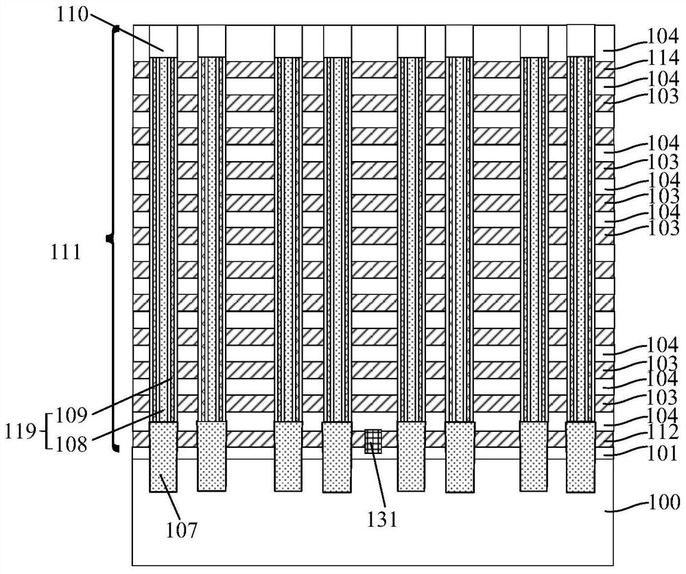
[0038] As mentioned in the background art, in the manufacturing process of the existing 3D NAND memory, the feature size of the gate spacers tends to fluctuate, which affects the performance of the memory.

[0039] It has been found through research that the side walls of the existing gate compartments are prone to inclination, so that the measured characteristic dimensions of the gate compartments tend to fluctuate.

[0040] Further studies have found that due to the large aspect ratio of the formed gate spacer, and after the formation of the gate spacer, the sacrificial layer in the stack structure will be removed, so that the strength of the stack structure is insufficient, which in turn makes the gate spacer The side walls of the groove are easily deformed or inclined. Moreover, since many manufacturing processes in the manufacturing process of 3D NAND memory are carried out at high temperature, the high temperature environment will cause deformation of the isolation layer...


PUM


Abstract

A 3D NAND memory and its forming method. The forming method of the 3D NAND memory of the present invention directly forms a stacked structure of a control gate and an isolation layer on a semiconductor substrate. After forming a storage structure in the stacked structure, etching In the top selection gate layer, the top selection gate layer is disconnected into several top selection gates, and the 3D NAND memory is correspondingly divided into several storage blocks through the disconnected top selection gates. Therefore, the 3D NAND memory storage of the present application Blocks are divided by disconnecting several top-layer select gates, and there is no need to form gate spacers in the stacked structure for the division of different memory blocks, thus avoiding fluctuations in the characteristic dimensions of the gate spacers and simplifying the process steps.

Description

technical field [0001] The invention relates to the field of semiconductor manufacturing, in particular to a method for reducing 3D NAND memory. Background technique [0002] NAND flash memory is a non-volatile storage product with low power consumption, light weight and good performance, and has been widely used in electronic products. At present, the NAND flash memory with a planar structure is close to the limit of practical expansion. In order to further increase the storage capacity and reduce the storage cost per bit, a 3D NAND memory with a 3D structure is proposed. [0003] The formation process of the existing 3D NAND memory generally includes: forming a stacked structure in which isolation layers and sacrificial layers are alternately stacked on the substrate; etching the stacked structure, forming channel vias in the stacked structure, and forming channel vias Finally, etch the substrate at the bottom of the channel via hole to form a groove in the substrate; in ...

Claims


Application Information

Patent Timeline
Patent Type & Authority Patents(China)
IPC IPC(8): H01L27/1157H01L27/11578H10B43/35H10B43/20
CPCH10B43/35H10B43/20H10B41/10H10B41/27H10B43/10H10B43/27
Inventor 霍宗亮欧文杨号号徐伟严萍黄攀周文斌
Owner YANGTZE MEMORY TECH CO LTD
Features
  • R&D
  • Intellectual Property
  • Life Sciences
  • Materials
  • Tech Scout
  • Unparalleled Data Quality
  • Higher Quality Content
  • 60% Fewer Hallucinations
Learn More