Display substrate, manufacturing method thereof, and display device

A display substrate, silicon-based technology, applied in the direction of diodes, organic semiconductor devices, semiconductor devices, etc., can solve problems such as short circuit between cathode and anode, and achieve the requirements of reducing production costs, improving product yield, and ensuring surface flatness and uniformity Effect

Active Publication Date: 2022-04-08
BOE TECH GRP CO LTD
View PDF7 Cites 0 Cited by
  • Summary
  • Abstract
  • Description
  • Claims
  • Application Information

AI Technical Summary

Problems solved by technology

[0005] The technical problem to be solved by the embodiments of the present invention is to provide a display substrate, its preparation method, and a display device, so as to solve the problem of a short circuit between the cathode and the anode in the preparation process of the existing silicon-based OLED microdisplay.

Method used


Image

  • Display substrate, manufacturing method thereof, and display device
  • Display substrate, manufacturing method thereof, and display device
  • Display substrate, manufacturing method thereof, and display device

Examples


Embodiment Construction

[0062] The specific implementation manners of the present invention will be further described in detail below in conjunction with the accompanying drawings and examples. The following examples are used to illustrate the present invention, but are not intended to limit the scope of the present invention. It should be noted that, in the case of no conflict, the embodiments in the present application and the features in the embodiments can be combined arbitrarily with each other.

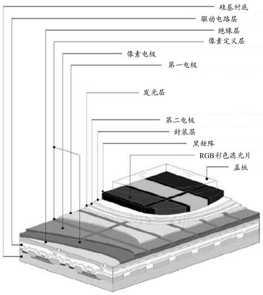
[0063] figure 1 It is a structural schematic diagram of an existing silicon-based OLED microdisplay. At present, when OLED is used as a micro-display, the way to achieve full color is to use white light + color film. Such as figure 1 As shown, the main structure of the silicon-based OLED microdisplay includes: a silicon-based substrate, a driving circuit layer, a light emitting structure layer, an encapsulation layer, a color filter layer and a cover plate. Among them, the silicon-based substrate i...


PUM


Abstract

The invention provides a display substrate, a preparation method thereof, and a display device. The display substrate includes a stacked microcavity structure layer and a light-emitting structure layer. Reflective electrodes are arranged in the microcavity structure layer, grooves are arranged on the surface of the microcavity structure layer, and the light-emitting structure layer includes The first electrode in the groove is connected to the reflective electrode. The present invention forms a groove on the microcavity structure layer, and the first electrode of the light emitting structure layer is arranged in the groove, effectively controlling the gap between the first electrode and the microcavity structure layer, and not only solves the problem of existing silicon-based There is a short-circuit problem between the cathode and the anode in the preparation process of the OLED microdisplay, and the surface flatness and uniformity requirements of the subsequent evaporation are guaranteed.

Description

technical field [0001] The invention relates to the field of display technology, in particular to an organic light-emitting display substrate, a preparation method thereof, and a display device. Background technique [0002] Microdisplays have a broad market application space, and are especially suitable for use in helmet-mounted displays, stereoscopic display mirrors, and eye-type displays. Microdisplay is in the interdisciplinary field of microelectronics technology and optoelectronics technology, involving a wide range of technologies, including optoelectronics, microelectronics, electronic informatics and optics, etc. technical field. Among them, the silicon-based OLED microdisplay, which combines Organic Light Emitting Diode (OLED) technology and Complementary Metal Oxide Semiconductor (CMOS) technology, is a cross-integrated product of the optoelectronics industry and the microelectronics industry. It can not only promote the development of a new generation of micro-...

Claims


Application Information

Patent Timeline
Patent Type & Authority Patents(China)
IPC IPC(8): H01L27/32
CPCH10K59/122H10K59/123H10K59/1213H10K59/32H10K59/38H10K59/124H10K50/818H10K50/852H10K2102/3026H10K2102/341H10K2102/351H10K50/814H10K59/1201
Inventor 杨盛际陈小川王辉黄冠达卢鹏程赵云翠谢东妹
Owner BOE TECH GRP CO LTD
Why Eureka
Try Eureka