Photosensitive component, imaging module, intelligent terminal, method and mold for manufacturing photosensitive component

A technology of photosensitive components and photosensitive elements, applied in semiconductor/solid-state device parts, image communications, electrical components, etc., can solve problems such as affecting installation and use, inability to accommodate glue, and oversize, etc., to strengthen the lateral bonding strength and facilitate the The effect of automatic alignment and stabilization of external dimensions

Active Publication Date: 2022-02-22
NINGBO SUNNY OPOTECH CO LTD
View PDF10 Cites 0 Cited by
  • Summary
  • Abstract
  • Description
  • Claims
  • Application Information

AI Technical Summary

Problems solved by technology

On the one hand, the glue has a certain fluidity. When the lens or motor and other components are installed after the glue is applied, the glue at the bottom of the component will overflow in all directions under pressure. At the same time, the applied glue needs to form a closed ring. The upper edge of the molding part is completely flat, relying only on the beveled or vertical edge of the draft cannot accommodate a large amount of glue overflowing from the starting point of the glue, the excess glue will overflow to the side of the module and protrude outward, making the size of the module Beyond the design range, affecting installation and use

Method used


Image

  • Photosensitive component, imaging module, intelligent terminal, method and mold for manufacturing photosensitive component
  • Photosensitive component, imaging module, intelligent terminal, method and mold for manufacturing photosensitive component
  • Photosensitive component, imaging module, intelligent terminal, method and mold for manufacturing photosensitive component

Examples


Embodiment Construction

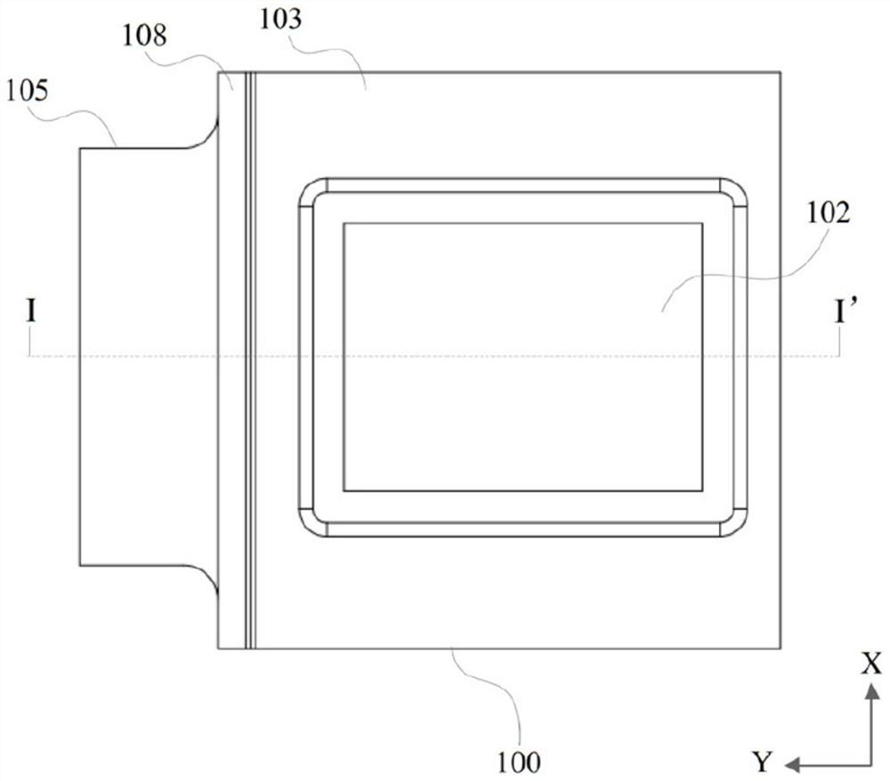
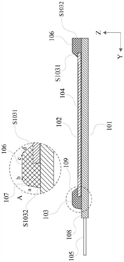
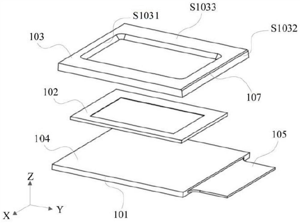
[0051] For a better understanding of the application, various aspects of the application will be described in more detail with reference to the accompanying drawings. It should be understood that these detailed descriptions are descriptions of exemplary embodiments of the application only, and are not intended to limit the scope of the application in any way. Throughout the specification, the same reference numerals refer to the same elements. The expression "and / or" includes any and all combinations of one or more of the associated listed items.

[0052] It should be noted that in this specification, expressions of first, second, etc. are only used to distinguish one feature from another, and do not represent any limitation on the features. Accordingly, a first body discussed hereinafter may also be referred to as a second body without departing from the teachings of the present application.

[0053] In the drawings, the thickness, size and shape of objects have been slight...


PUM


Abstract

A photosensitive component, an imaging module, an intelligent terminal, and a method and a mold for manufacturing the photosensitive component are disclosed. The photosensitive assembly includes: a circuit board, a hard board area having a rectangular shape and a soft board extension extending from the hard board area, wherein the hard board area has a pressing side and a non-pressing side, and the hard board area has a pressing side on the pressing side a pressing area; a photosensitive element mounted in the hard board area of ​​the circuit board; and a molding part formed on the hard board area, surrounding the photosensitive element and extending towards the photosensitive element and contacting the photosensitive element, the molding part has an inner surface, an outer side surface and top surface, and the molding part does not cover the pressing area of ​​the hard board area, and the top surface has a flat part; wherein, the top surface of the part of the molding part on the pressing side has a settling part, and the settling part is located between the flat part and the mold part. The outer surfaces of the molded parts are between and lower than the flat part, and the outer surface of the part of the molded part on the non-pressed side is perpendicular to the flat part.

Description

[0001] Cross References to Related Applications [0002] This application claims the priority and benefit of Chinese patent applications No. 201710712589.1 and No. 201721042380.0 filed with the State Intellectual Property Office of China on August 18, 2017, the entire contents of which are incorporated herein by reference. technical field [0003] The present disclosure relates to the technical field of imaging components and intelligent terminals, in particular, to a photosensitive component, an imaging module, a smart terminal, a method and a mold for manufacturing a photosensitive component. Background technique [0004] Molded camera module is a high-tech that is very popular in the current market. Molding replaces the general lens holder, and the photosensitive chip, connection medium and electronic components of the camera module are covered and fixed on the circuit board. , obtained good impact stability and thermal stability. At the same time, the upper surface of t...

Claims


Application Information

Patent Timeline
Patent Type & Authority Patents(China)
IPC IPC(8): H04N5/225H01L23/31
CPCH01L23/3185H04N23/54H04N23/50H04N23/57H04N23/55
Inventor 田中武彦陈振宇梅哲文
Owner NINGBO SUNNY OPOTECH CO LTD
Why Eureka
Try Eureka