Open-drain output control circuit
A technology of output control and circuit, which is applied in the direction of control/regulation system, regulation of electrical variables, instruments, etc., can solve problems such as false triggering of FLAG output, and achieve the effect of avoiding false triggering of output and eliminating high-level faults
- Summary
- Abstract
- Description
- Claims
- Application Information
AI Technical Summary
Problems solved by technology
Method used
Image


Examples
Embodiment 1
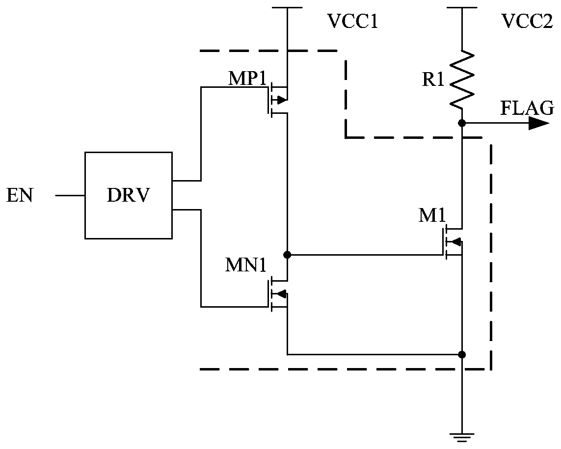
[0044] ginseng Figure 4 As shown, an open-drain output control circuit in a specific embodiment of the present invention includes:
[0045] The first MOS transistor MP1 and the second MOS transistor MN1 are electrically connected between the first power supply voltage VCC1 and the reference potential, the gates of the first MOS transistor MP1 and the second MOS transistor MN1 are connected to the DRV unit, and the DRV unit receives the first MOS transistor MN1. 1. Enable signal EN;
[0046] The first resistor R1 and the third MOS transistor M1 are electrically connected between the second power supply voltage VCC2 and the reference potential, and the gate of the third MOS transistor M1 is connected to the drains of the first MOS transistor MP1 and the second MOS transistor MN1 , the drain of the third MOS transistor M1 outputs the second enable signal FLAG;
[0047] The second resistor R2 is connected between the gate and the drain of the third MOS transistor M1, and is use...
Embodiment 2
[0061] ginseng Figure 8 As shown, an open-drain output control circuit in another specific embodiment of the present invention includes:
[0062] The first MOS transistor MP1 and the second MOS transistor MN1 are electrically connected between the first power supply voltage VCC1 and the reference potential, the gates of the first MOS transistor MP1 and the second MOS transistor MN1 are connected to the DRV unit, and the DRV unit receives the first MOS transistor MN1. 1. Enable signal EN;
[0063] The first resistor R1 and the third MOS transistor M1 are electrically connected between the second power supply voltage VCC2 and the reference potential, and the gate of the third MOS transistor M1 is connected to the drains of the first MOS transistor MP1 and the second MOS transistor MN1 , the drain of the third MOS transistor M1 outputs the second enable signal FLAG;
[0064] The second resistor R2 is connected between the gate and the drain of the third MOS transistor M1, and ...
PUM
 Abstract
Description
Claims
Application Information