Supercharge Your Innovation With Domain-Expert AI Agents!

Display device

A technology for display devices and display media, applied in the fields of optics, instruments, characters and pattern recognition, etc., can solve the problem of white point coordinate offset of the display panel, etc., and achieve the effect of improving the problem of white point coordinate offset

Active Publication Date: 2021-04-23
AU OPTRONICS CORP
View PDF5 Cites 0 Cited by
  • Summary
  • Abstract
  • Description
  • Claims
  • Application Information

AI Technical Summary

Problems solved by technology

However, when the sensing element layer is integrated in the display panel, the display light beam used to display the image needs to pass through the sensing element layer before being delivered to human eyes, causing the coordinates of the white point of the display panel to shift.

Method used


Image

  • Display device
  • Display device
  • Display device

Examples


Embodiment Construction

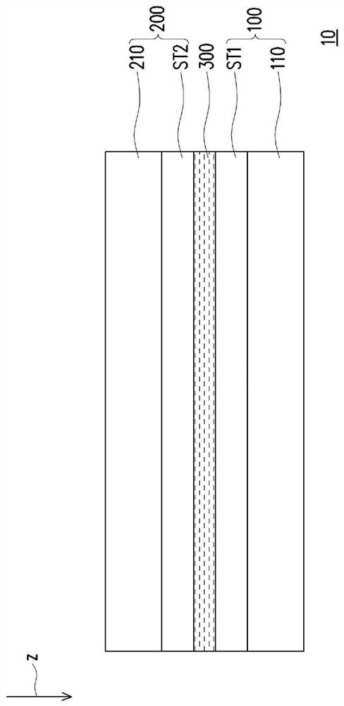
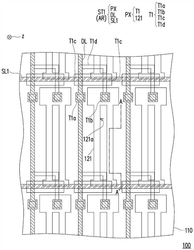
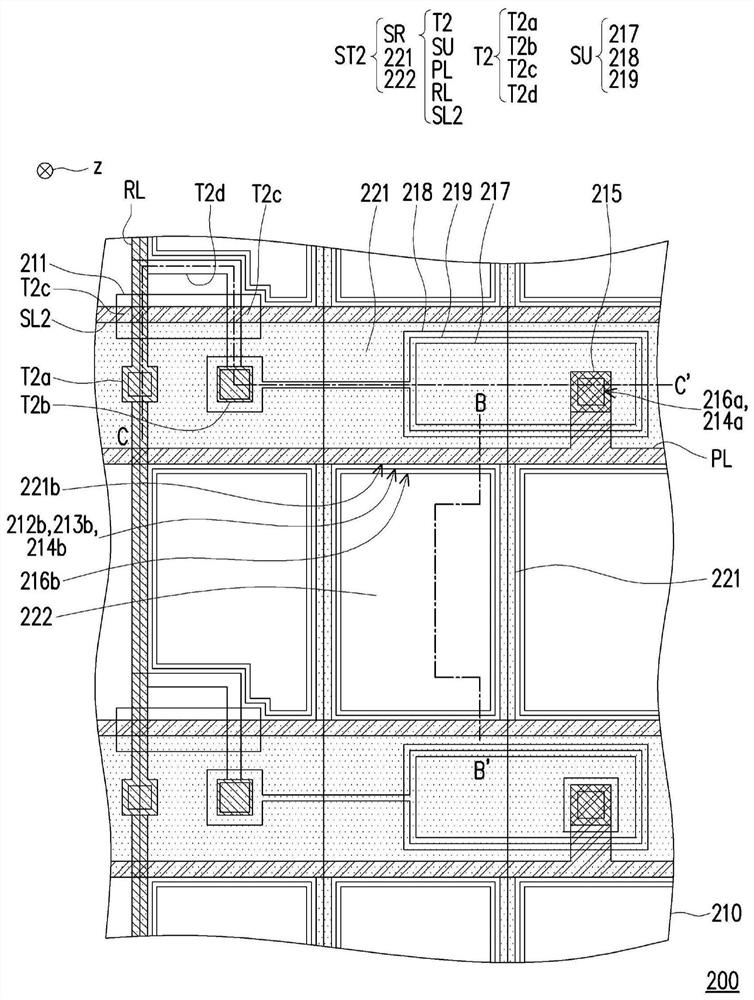
[0064] Reference will now be made in detail to the exemplary embodiments of the present invention, examples of which are illustrated in the accompanying drawings. Wherever possible, the same reference numbers will be used in the drawings and description to refer to the same or like parts.

[0065] It will be understood that when an element such as a layer, film, region, or substrate is referred to as being "on" or "connected to" another element, it can be directly on or connected to the other element, or Intermediate elements may also be present. In contrast, when an element is referred to as being "directly on" or "directly connected to" another element, there are no intervening elements present. As used herein, "connected" may refer to physical and / or electrical connection. Furthermore, "electrically connected" or "coupled" may mean that other elements exist between two elements.

[0066] As used herein, "about," "approximately," or "substantially" includes stated values ...


PUM


Abstract

The invention provides a display device. The display device comprises a first substrate, a second substrate, a display medium, a pixel structure, a reading transistor, a first insulating layer, a photosensitive structure and a color filter pattern. The second substrate is disposed opposite to the first substrate. The display medium is disposed between the first substrate and the second substrate. The pixel structure is arranged between the display medium and the first substrate. The reading transistor has a semiconductor pattern and a control terminal. The photosensitive structure is disposed between the second substrate and the display medium, and is electrically connected to the reading transistor. The first insulating layer is disposed between the semiconductor pattern of the reading transistor and the control terminal. The color filter pattern is disposed between the second substrate and the display medium. The first insulating layer is provided with an opening located outside the photosensitive structure, and the color filter pattern is filled in the opening of the first insulating layer. In addition, another display device is also provided.

Description

technical field [0001] The invention relates to a display device. Background technique [0002] Today's electronic devices (such as mobile phones) are equipped with biometric technology to enhance privacy and data protection capabilities has become a mainstream function. Common biometric identification technologies include ultrasonic fingerprint recognition sensing, optical fingerprint recognition sensing, capacitive fingerprint recognition sensing, face recognition, etc. Among them, the optical fingerprint sensing technology is easily integrated into the display panel process. The sensing element layer is used to detect the light beam reflected by the fingerprint, and then obtain the fingerprint image. However, when the sensing element layer is integrated in the display panel, the display light beam used to display the image needs to pass through the sensing element layer before being delivered to human eyes, causing the white point coordinates of the display panel to shif...

Claims


Application Information

Patent Timeline
Patent Type & Authority Applications(China)
IPC IPC(8): G06K9/00G02F1/1333
CPCG02F1/133514G02F1/13312G02F1/1368G02F1/136227G02F1/136209G02F1/136222G02F1/13338
Inventor 苏志中陈信学陈亦伟
Owner AU OPTRONICS CORP
Features
  • R&D
  • Intellectual Property
  • Life Sciences
  • Materials
  • Tech Scout
  • Unparalleled Data Quality
  • Higher Quality Content
  • 60% Fewer Hallucinations
Learn More