Chip transfer method and display device

A chip transfer, chip technology, applied in the identification of devices, instruments, electrical components, etc., can solve problems such as chip transfer failure, and achieve the effect of ensuring successful transfer.

Active Publication Date: 2021-06-15
CHONGQING KONKA PHOTOELECTRIC TECH RES INST CO LTD
View PDF8 Cites 3 Cited by
  • Summary
  • Abstract
  • Description
  • Claims
  • Application Information

AI Technical Summary

Problems solved by technology

[0004] In view of the above deficiencies in the prior art, the purpose of this application is to provide a chip transfer method and a disp

Method used


Image

  • Chip transfer method and display device
  • Chip transfer method and display device
  • Chip transfer method and display device

Examples


Example Embodiment

[0031] In order to facilitate the understanding of the present application, the present application will be described more fully below with reference to the relevant drawings. Preferred embodiments of the application are shown in the accompanying drawings. However, the present application can be embodied in many different forms and is not limited to the embodiments described herein. On the contrary, the purpose of providing these embodiments is to make the disclosure of the application more thorough and comprehensive.

[0032] Unless otherwise defined, all technical and scientific terms used herein have the same meaning as commonly understood by one of ordinary skill in the technical field to which this application belongs. The terminology used herein in the description of the application is only for the purpose of describing specific embodiments, and is not intended to limit the application.

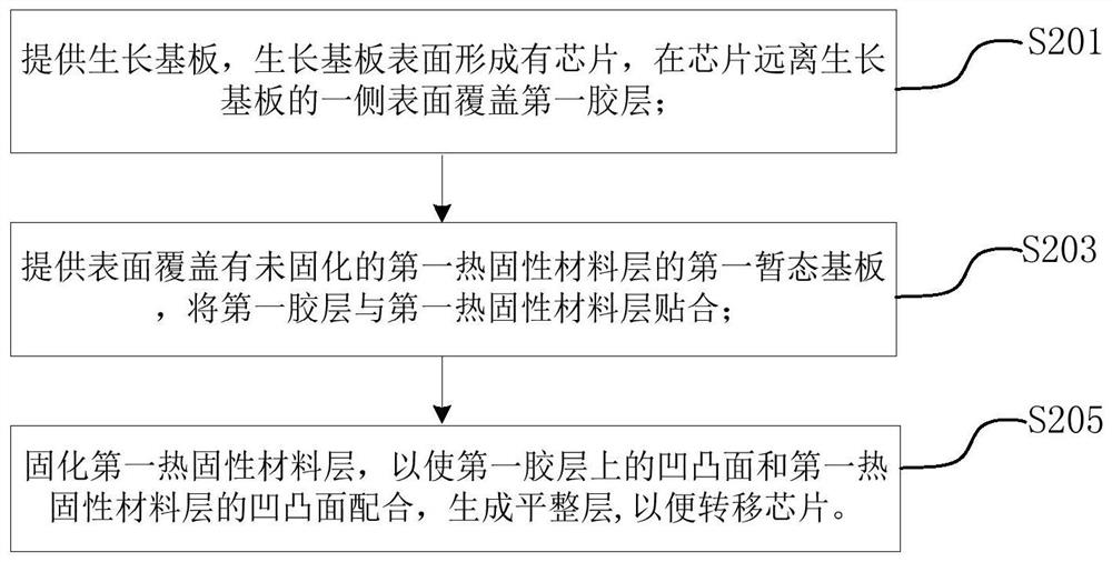
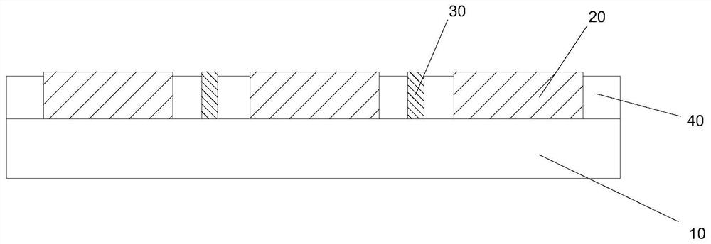
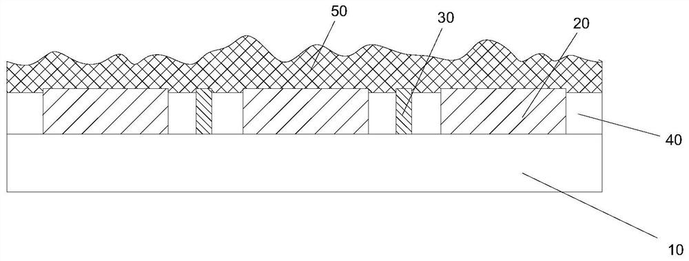
[0033] As described in the background technology section, in the process of reali...


PUM


Abstract

The invention relates to a chip transfer method and a display device. The chip transfer method comprises the following steps that: a growth substrate is provided, a chip is formed on the surface of the growth substrate, and the surface of the side, away from the growth substrate, of the chip is covered with a first adhesive layer; a first transient substrate of which the surface is covered with an uncured first thermosetting material layer is provided, and the first adhesive layer is attached to the first thermosetting material layer; and the first thermosetting material layer is cured, so that a concave-convex surface on the first adhesive layer can be matched with a concave-convex surface of the first thermosetting material layer to generate a flat layer, so that the chip can be transferred. According to the chip transfer method, the situation that some chips are not completely attached or sink into a glue material on the surface of another temporary substrate due to insufficient height in the pressure attachment transfer process of the chips and the other substrate is avoided, and successful transfer of the chips is guaranteed.

Description

technical field [0001] The invention relates to the field of display technology, in particular to a chip transfer method and a display device. Background technique [0002] At present, a key technology facing the chip transfer technology is to transfer the chip to the display backplane through the mass transfer process. substrate, and then transfer the chip from the first temporary substrate to the second temporary substrate by a similar method, and then transfer and bind the chip from the second temporary substrate to the backplane. [0003] However, in the process of realizing chip transfer in the prior art, since the adhesive material coated on the temporary substrate is fluid before curing, there are often differences in thickness after curing, so that in the process of pressure bonding with another substrate , due to the difference in the height of the adhesive material, some chips will be adhered under normal pressure, while some chips will be incompletely adhered due...

Claims


Application Information

Patent Timeline
IPC IPC(8): H01L33/48H01L21/683G09F9/33
CPCH01L21/6835H01L33/48G09F9/33H01L2221/68368
Inventor 蒲洋洪温振
Owner CHONGQING KONKA PHOTOELECTRIC TECH RES INST CO LTD
Why Eureka
Try Eureka