Display panel

A technology for display panels and substrates, which is applied to semiconductor devices, electrical components, circuits, etc., can solve the problems of lowering the display performance of light-emitting devices, and achieve the effects of reducing leakage current and improving stability.

Pending Publication Date: 2022-05-06
SHENZHEN CHINA STAR OPTOELECTRONICS SEMICON DISPLAY TECH CO LTD
View PDF0 Cites 1 Cited by
  • Summary
  • Abstract
  • Description
  • Claims
  • Application Information

AI Technical Summary

Problems solved by technology

[0002] Due to the light-sensitive characteristics of semiconductor materials, the characteristics of semiconductor materials of thin-film transistors are affected by external ambient light and light emitted by light-emitting devices, resulting in reduced display performance of light-emitting devices driven by thin-film transistors

Method used


Image

  • Display panel
  • Display panel
  • Display panel

Examples


Embodiment Construction

[0027] The technical solutions in the embodiments of the present application will be clearly and completely described below in conjunction with the drawings in the embodiments of the present application. Apparently, the described embodiments are only some of the embodiments of this application, not all of them. Based on the embodiments in this application, all other embodiments obtained by those skilled in the art without making creative efforts belong to the scope of protection of this application.

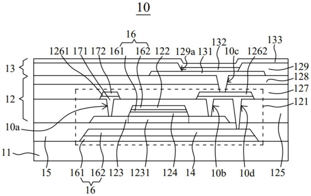
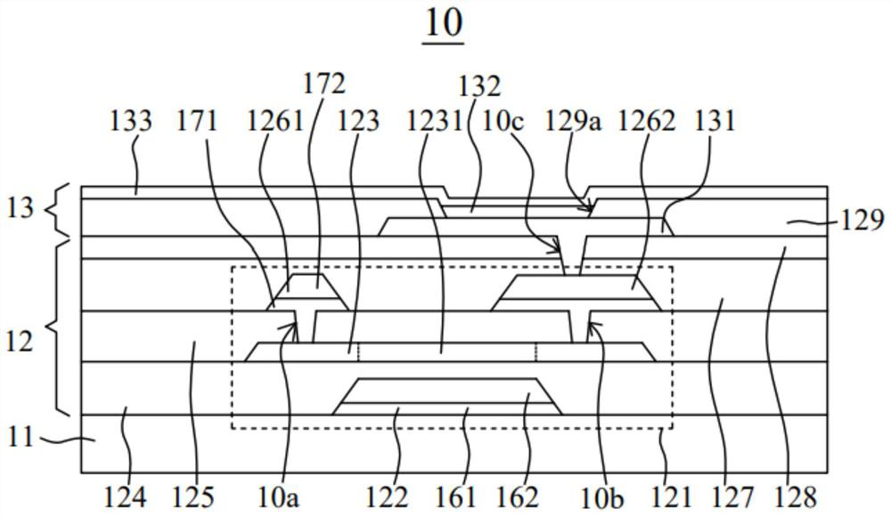
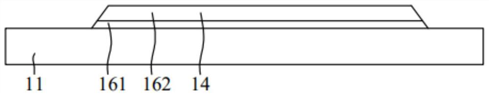
[0028] Such as figure 1 As shown, it is a schematic diagram of the display panel according to the first embodiment of the present application. The display panel 10 includes a substrate 11 , a thin film transistor array layer 12 , a light emitting device layer 13 , a light shielding layer 14 and a buffer layer 15 .

[0029] In this embodiment, the substrate 11 is a glass substrate. In other embodiments, the substrate 11 may also be a flexible substrate.

[0030] In this embodi...


PUM


Abstract

The invention provides a display panel. The display panel comprises a substrate; the thin film transistor is arranged on one side of the substrate, the thin film transistor comprises an active layer, and the active layer comprises a channel; the shading conductive layer is arranged in the thickness direction of the display panel, the shading conductive layer and a channel of the active layer are overlapped, and the shading conductive layer comprises a first light absorption layer; and the first conductive layer is positioned on one side, far away from the substrate, of the first light absorption layer.

Description

technical field [0001] The present application relates to the field of display technology, and in particular to a display panel. Background technique [0002] Due to the light-sensitive characteristic of the semiconductor material, the characteristics of the semiconductor material of the thin film transistor are affected by the external ambient light and the light emitted by the light emitting device, resulting in a decrease in the display performance of the light emitting device driven by the thin film transistor. [0003] Therefore, it is necessary to propose a technical solution to solve the influence of light on the semiconductor material of the thin film transistor. Contents of the invention [0004] The purpose of the present application is to provide a display panel to improve the effect of light on the active layer of the thin film transistor. [0005] In order to achieve the above object, the technical scheme is as follows: [0006] A display panel comprising: ...

Claims


Application Information

Patent Timeline
IPC IPC(8): H01L27/32
CPCH10K59/123H10K59/124H10K59/1213H10K59/126
Inventor 林高波
Owner SHENZHEN CHINA STAR OPTOELECTRONICS SEMICON DISPLAY TECH CO LTD
Why Eureka
Try Eureka