Integrated circuit device and processing method thereof, electronic equipment and board card

A technology of integrated circuits and processing methods, which is applied in the direction of circuits, electrical components, and electrical solid devices, can solve problems such as poor flexibility and scalability, and the inability to fully utilize the die-to-die interface, so as to improve competitiveness and expand Effects of storage bandwidth and capacity, optimal operational performance

Pending Publication Date: 2022-05-13
ANHUI CAMBRICON INFORMATION TECH CO LTD
View PDF0 Cites 0 Cited by
  • Summary
  • Abstract
  • Description
  • Claims
  • Application Information

AI Technical Summary

Problems solved by technology

Although such a chip design and packaging method improves the yield rate of the chip and reduces the cost of the entire product to some extent, in some application scenarios, this method has poor flexibility and scalability in layout, and also Inability to fully utilize the die-to-die interface used to interconnect chips

Method used


Image

  • Integrated circuit device and processing method thereof, electronic equipment and board card
  • Integrated circuit device and processing method thereof, electronic equipment and board card
  • Integrated circuit device and processing method thereof, electronic equipment and board card

Examples


Embodiment Construction

[0018] The following will clearly and completely describe the technical solutions in the embodiments of the present disclosure with reference to the drawings in the embodiments of the present disclosure. Obviously, the described embodiments are part of the embodiments of the present disclosure, not all of them. Based on the embodiments in the present disclosure, all other embodiments obtained by those skilled in the art without creative efforts fall within the protection scope of the present disclosure.

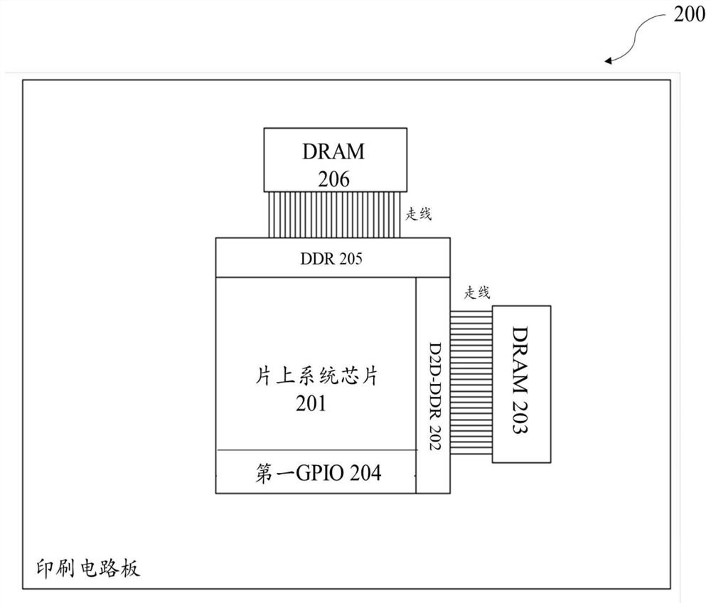
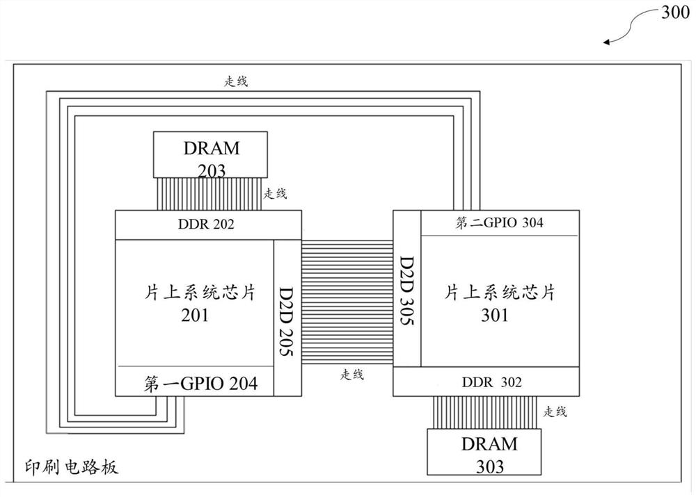
[0019] The following will be combined with Figure 1-6 The details of various embodiments of the present disclosure will be described in detail.

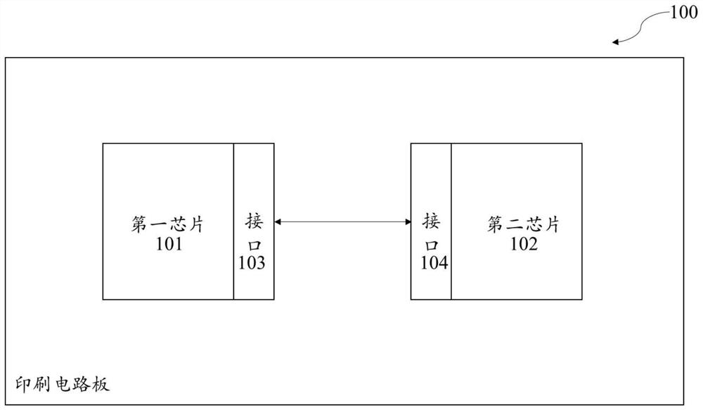
[0020] figure 1 is a schematic structural diagram showing the integrated circuit device 100 according to an embodiment of the present disclosure. like figure 1 As shown, the integrated circuit device 100 may include a printed circuit board (Printed Circuit Board, “PCB”), and a first chip 101 and a second chip 102 are arranged on...


PUM


Abstract

The present disclosure relates to an integrated circuit device, a processing method thereof, an electronic device, and a board card wherein the integrated circuit device can be implemented in a combined processing device which can include a computing processing device and other processing devices. And the computing processing device interacts with other processing devices so as to jointly complete computing operation specified by a user. The combined processing device can further comprise a storage device, and the storage device is connected with the calculation processing device and the other processing devices and used for storing data of the calculation processing device and the other processing devices in some application scenes. According to the scheme disclosed by the invention, interconnection and mutual access of a pipe core level and interface multiplexing can be realized, and the storage bandwidth and capacity are also expanded in some application scenarios.

Description

technical field [0001] The present disclosure relates generally to the field of circuits. More specifically, the present disclosure relates to an integrated circuit device and its processing method, electronic equipment and board. Background technique [0002] Currently, in chip design, various functions expected to be obtained can be divided so as to be respectively realized by two or more small-sized chips. Based on this, after each small chip is designed and produced separately, multiple small chips are sealed together through the packaging process. Although such a chip design and packaging method improves the yield rate of the chip and reduces the cost of the entire product to some extent, in some application scenarios, this method has poor flexibility and scalability in layout, and also The die-to-die interface used to interconnect chips cannot be fully utilized. Contents of the invention [0003] In view of at least the above technical problems, the present disclo...

Claims


Application Information

Patent Timeline
Patent Type & Authority Applications(China)
IPC IPC(8): H01L25/18H01L23/498H01L21/48
CPCH01L25/18H01L23/49838H01L21/4875
Inventor 不公告发明人
Owner ANHUI CAMBRICON INFORMATION TECH CO LTD
Why Eureka
Try Eureka