Semiconductor module

A semiconductor and main body technology, applied in semiconductor devices, electric solid state devices, instruments, etc., can solve the problem of increasing noise chips, and achieve the effects of reducing power consumption, improving data transmission efficiency, and expanding storage bandwidth

Active Publication Date: 2020-01-24
ULSTREETCAREMORY INC
View PDF10 Cites 0 Cited by
  • Summary
  • Abstract
  • Description
  • Claims
  • Application Information

AI Technical Summary

Problems solved by technology

On the other hand, this increase in capacity has reached its limit due to vulnerability to noise due to miniaturization, increase in die area, etc.

Method used


Image

  • Semiconductor module
  • Semiconductor module
  • Semiconductor module

Examples


Embodiment Construction

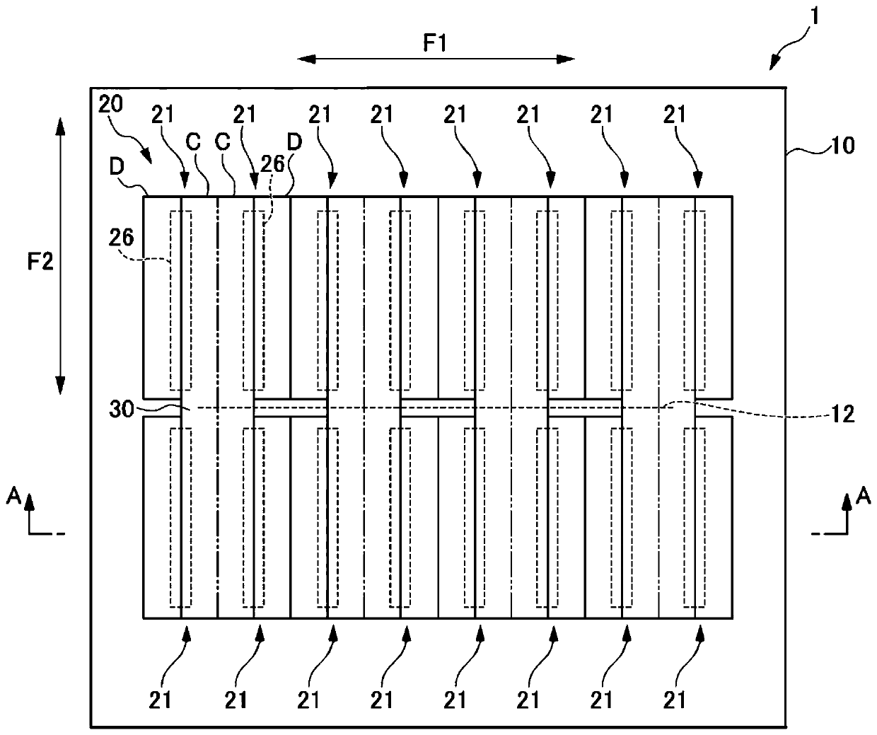
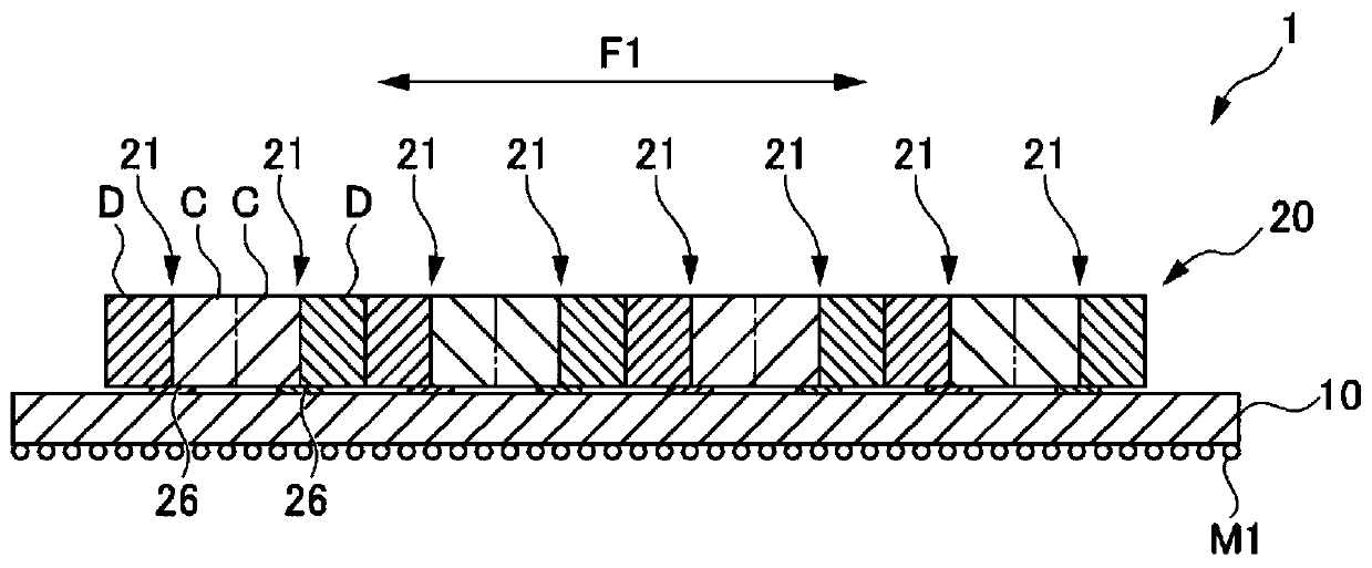
[0026] Hereinafter, a semiconductor module according to an embodiment of the present invention will be described with reference to the drawings.

[0027] The semiconductor module 1 of the present embodiment is, for example, a SIP (system in a package: system in package) in which an arithmetic unit (hereinafter referred to as an MPU) and a stacked DRAM are arranged on an interposer. The semiconductor module 1 is disposed on another interposer or packaging substrate, and is electrically connected using micro bumps. The semiconductor module 1 is a device that obtains power from another interposer or package substrate and can transmit and receive data to and from another interposer or package substrate.

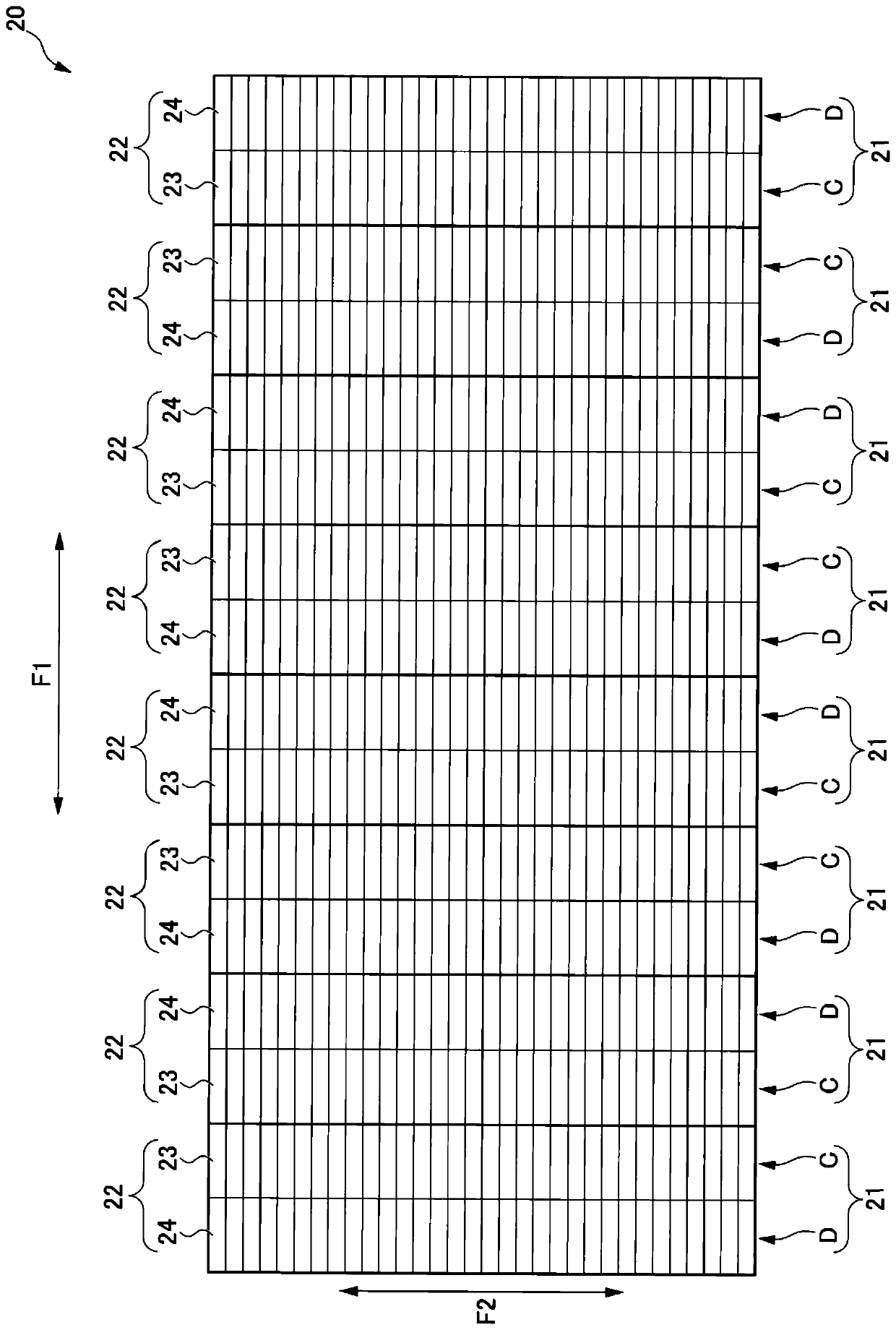
[0028] Such as figure 1 and figure 2 As shown, the semiconductor module 1 has an interposer 10 and a processing part 20 .

[0029] The interposer 10 is formed in a plate shape, and the surface on one side of the interposer is electrically connected to another interposer or a ...


PUM

PropertyMeasurementUnit
lengthaaaaaaaaaa

Abstract

Provided is a semiconductor module which enables a memory bandwidth to be widened, and which enables data transfer efficiency to be improved by reducing power consumption. A semiconductor module (1) comprises: an interposer (10); and a processing unit (20) which has a plurality of processing unit bodies (21) arrayed to be side by side with each other in a first direction (F1) along the sheet surface of the interposer (10), and which is placed on the interposer (10) so as to be electrically connected to the interposer (10). The processing unit bodies (21) are provided with a plurality of subsetunits (22) each including: one calculation unit (23) including at least one core (25); and one memory unit (24) that is configured from a stacked-type RAM module and that is disposed to be side by side with the calculation unit (23) in the first direction (F1). The plurality of subset units (22) are arrayed to be side by side with each other in a second direction (F2) that intersects with the first direction (F1).

Description

technical field [0001] The invention relates to semiconductor modules. Background technique [0002] Conventionally, volatile memories such as DRAM (Dynamic Random Access Memory: Dynamic Random Access Memory) are known as storage devices. The DRAM is required to have a large capacity that can withstand an increase in the amount of data corresponding to an increase in the performance of a computing device (hereinafter referred to as an MPU). Therefore, there has been an ongoing pursuit of increasing the capacity of memories (memory cell arrays, memory chips) through miniaturization and planar expansion of cells. On the other hand, such increase in capacity has reached its limit due to the vulnerability to noise due to miniaturization, increase in die area, and the like. [0003] Therefore, recently, a technique of stacking a plurality of planar memories to achieve a three-dimensional (3D) increase in capacity has been proposed (for example, refer to Patent Documents 1 to 4)...

Claims


Application Information

Patent Timeline
Patent Type & Authority Applications(China)
IPC IPC(8): G11C5/02G06F12/00G11C5/04H01L25/065H01L25/07H01L25/16H01L25/18
CPCG11C5/04G11C5/063H01L25/0652H01L2924/15311H01L24/08H01L24/16H01L2224/16227H01L2224/08225H01L24/80H01L2224/80905H01L2224/80895H01L2224/80896H01L24/83H01L2224/83851H01L24/32H01L2224/32227H01L2224/83101H01L2924/00014G06F1/02
Inventor 梶谷一彦安达隆郎
Owner ULSTREETCAREMORY INC
Why Eureka
Try Eureka