memory structure

A technology of memory bank and topology structure, applied in the computer field, can solve the problems such as the inability to increase the memory access bandwidth, the reduction of the bandwidth, and the increase of the signal rate.

Active Publication Date: 2015-08-12
JIANGNAN INST OF COMPUTING TECH
View PDF4 Cites 0 Cited by
  • Summary
  • Abstract
  • Description
  • Claims
  • Application Information

AI Technical Summary

Problems solved by technology

[0008] 2. Double RANK will add a small number of address group signals, in which the number of clock and control signals is doubled and the topology of 1 push 9 Fly-by is maintained. The number of address and command signals remains unchanged but the load is increased to 1 push 18 Fly-by topology. Aggravation has an impact on the quality of signal transmission and affects the efficiency of memory access
[0009] 3. The number of signals in the address group of the dual RANK remains unchanged, but the topology changes from point-to-point to 1 push 2. The increased load will affect the quality of signal transmission and the increase of signal rate (may lead to a decrease in bandwidth)
[0016] However, high-speed memory chips are an inevitable choice for high-performance computing, so the above method only has a limited effect on increasing the assembly density, and cannot effectively increase the memory access bandwidth while increasing the assembly density.

Method used


Image

  • memory structure
  • memory structure
  • memory structure

Examples


no. 1 example

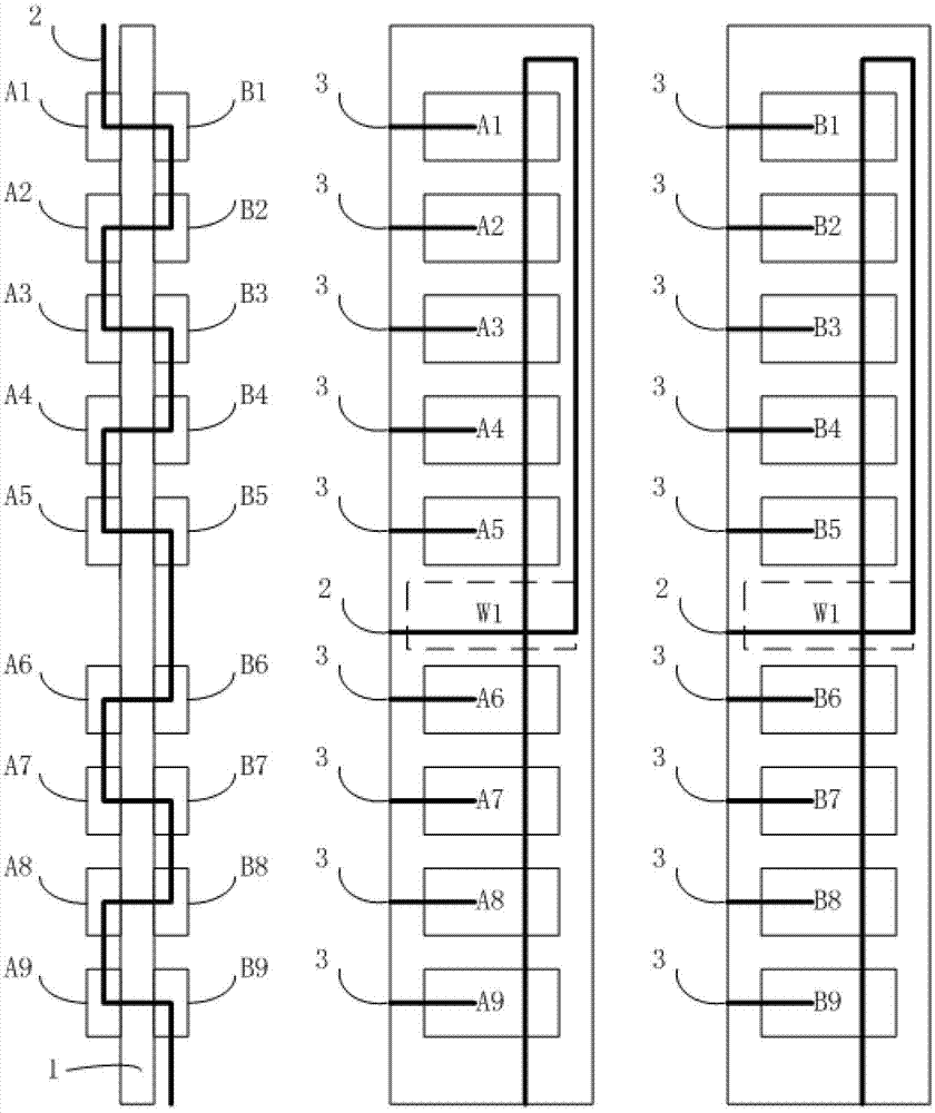
[0035] figure 2 It schematically shows the front arrangement, the back arrangement, and the signal connection relationship of the memory structure according to the embodiment of the present invention.

[0036] Such as figure 2 As shown, nine front storage body units are arranged side by side on the front side of the printed board 1: the first front storage unit A1, the front second storage unit A2, the front third storage unit A3, and the front fourth storage unit A4, the fifth bank unit A5 on the front side, the sixth bank unit A6 on the front side, the seventh bank unit A7 on the front side, the eighth bank unit A8 on the front side, and the ninth bank unit A9 on the front side.

[0037] On the opposite side of the printed board, at positions corresponding to the nine front memory cells, nine reverse memory cells are arranged side by side: the first memory cell unit B1 on the reverse side, the second memory cell unit B2 on the reverse side, and the second memory cell unit...

no. 2 example

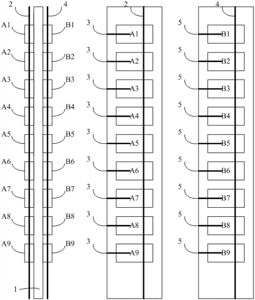
[0047] Preferably, a part of the nine front memory units is arranged in the first front row, and the rest of the nine front memory units are arranged in the second front row, and the arrangement direction of the first front row is the same as that of the front first row. The arrangement direction of the second row of the front side is vertical; and, a part of the nine back memory body units is arranged in the first row of the back side, and the rest of the nine back memory body units are arranged in the second row of the back side, the The arrangement direction of the first row on the reverse side is perpendicular to the arrangement direction of the second row on the reverse side.

[0048] The following will combine image 3 A specific example of such a preferred embodiment will be described.

[0049] image 3 Schematically shows another arrangement of the memory structure according to the embodiment of the present invention; it shows a right-angle turning layout, and its si...

no. 3 example

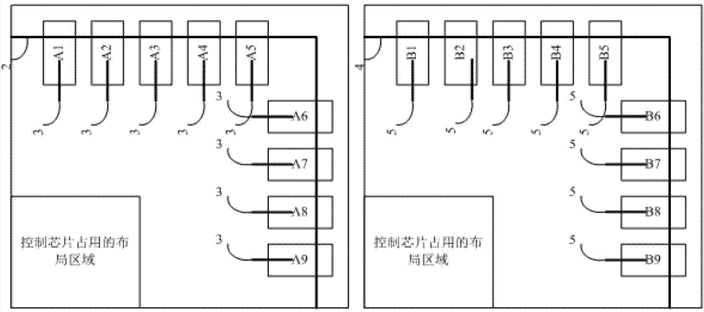
[0059] Preferably, a part of the nine front memory units is arranged in the first front row, and the rest of the nine front memory units are arranged in the second front row, and the arrangement direction of the first front row is the same as that of the front first row. The arrangement direction of the second row of the front side is parallel; and, a part of the nine backside memory cells is arranged in the first row of the backside, and the rest of the nine backside memory body units are arranged in the second row of the backside, and the The arrangement direction of the first row on the opposite side is parallel to the arrangement direction of the second row on the opposite side.

[0060] The following will combine Figure 4 A specific example of such a preferred embodiment will be described. Figure 4 Schematically shows another arrangement of the memory structure according to the embodiment of the present invention; it shows the layout form of the horizontal transition, ...


PUM


Abstract

The invention discloses a storage body structure. Nine front-surface storage body units, namely a front-surface first storage body unit, a front-surface second storage body unit, a front-surface third storage body unit, a front-surface fourth storage body unit, a front-surface fifth storage body unit, a front-surface sixth storage body unit, a front-surface seventh storage body unit, a front-surface eighth storage body unit and a front-surface ninth storage body unit, are arranged on the front surface of a printed plate side by side. Nine back-surface storage body units, namely a back-surface first storage body unit, a back-surface second storage body unit, a back-surface third storage body unit, a back-surface fourth storage body unit, a back-surface fifth storage body unit, a back-surface sixth storage body unit, a back-surface seventh storage body unit, a back-surface eighth storage body unit and a back-surface ninth storage body unit, are arranged at the positions, opposite to the front-surface storage body units, of the back surface of the printed plated side by side. The nine front-surface storage body units arranged on the front surface of the printed circuit belong to a first path of storage control; and the nine back-surface storage body units arranged on the back surface of the printed circuit belong to a second path of storage control.

Description

technical field [0001] The present invention relates to computer technology, and more specifically, the present invention relates to a storage body structure and a storage body arrangement method. Background technique [0002] To date, memory banks built from various generations of memory chips have been an indispensable basic element in the field of high-performance computing. With the rapid development of high-performance processors, the relative lag of memory development has introduced the problem of "storage wall", which mainly includes storage depth (depending on storage bit width and single-bit storage density), storage bandwidth (depending on storage At the same time, high-performance computing itself has increasingly stringent requirements for memory assembly density. As an important fixed component of computing node layout, increasing the main memory layout density is conducive to improving the assembly density. . [0003] At present, the commercial memory standar...

Claims


Application Information

Patent Timeline
Patent Type & Authority Patents(China)
IPC IPC(8): G11C11/413
Inventor 王彦辉刘耀贾福桢金利峰李滔周培峰
Owner JIANGNAN INST OF COMPUTING TECH
Why Eureka
Try Eureka