If the DIP method is used, the circuit board needs to be provided with corresponding through holes, so that the multi-layer lines in the circuit board need to avoid the aperture and make the lines unable to be dense, so that the volume of the circuit board and electrical connectors cannot be reduced. As for the use of SMT And the BGA method, which requires that the lower surface of the
electrical connector solder feet or solder balls must maintain a fairly high coplanarity, otherwise it will cause a virtual
soldering between some solder legs or solder balls and the circuit board, resulting in the
electrical connector and the circuit board. The telecommunication connection line between them is interrupted and the predetermined function cannot be realized. Therefore, it is very important to detect the flatness of the above-mentioned solder feet or solder balls in the production process. At present, the detection method used in the industry is mainly by detecting the relative The height of the lower surface 15 of the electrical connector 10, and then compare all the measured values to get the difference between the highest value and the lowest value, and then compare the difference with the theoretical calculation to ensure that all
soldering pins and circuit boards can be welded Theoretical difference is compared to judge whether the
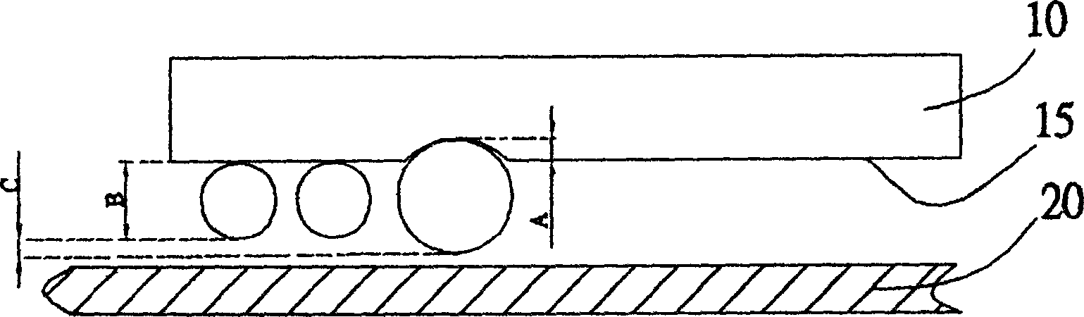
welding pin meets the coplanarity requirements, but the problems that may arise in this method are: 1) If figure 1 As shown, when the lower surface 15 of the electrical connector 10 connected to the highest soldering point is partially bent upwards and deformed, the measured height of the soldering leg arranged there is A+B+C (the bottom surface bent upwards of the lower surface 15 to The height of the top of the soldering pin), and the height of the most soldering pin is B, so the
height difference between the highest point and the lowest point is A+C, which may exceed the theoretical calculation to ensure that all soldering pins and the circuit board 20 can be welded. The difference leads to the judgment that the product is unqualified, but based on the lower surface of the electrical connector connected to the lowest soldering point, the
height difference between the two is C, which may be within the range of theoretical values to ensure that all soldering points can be contact with the circuit board
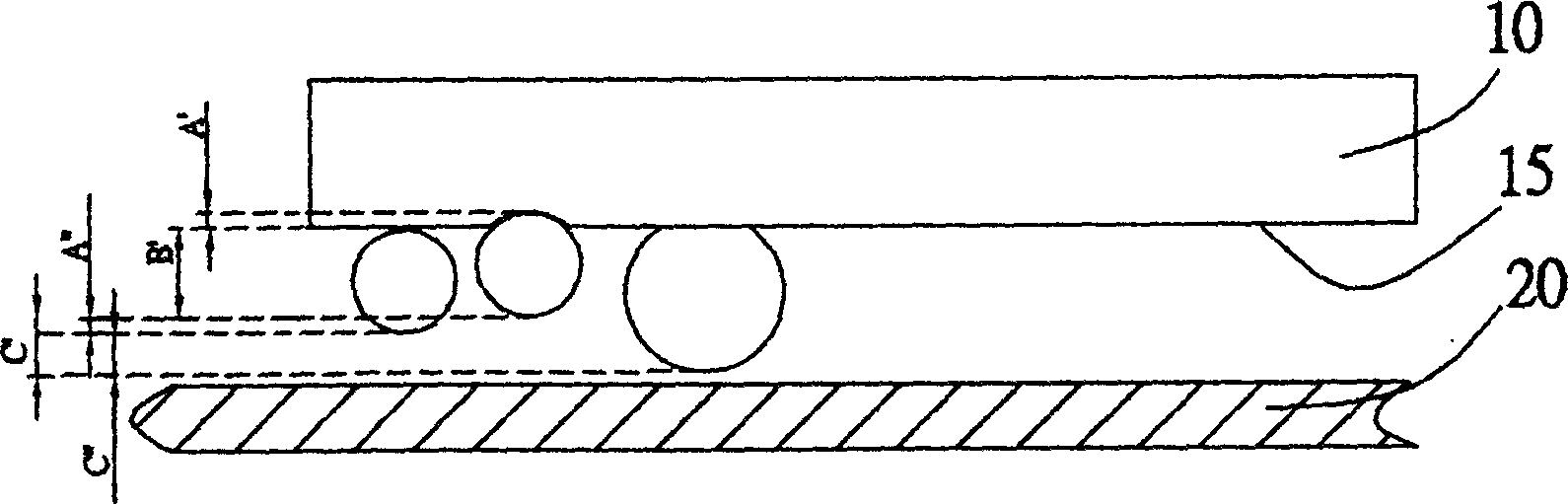
Another situation such as figure 2 As shown, when the lower surface 15 of the electrical connector 10 at the lowest soldering point is locally bent and deformed, the height of the lowest soldering point is A'+B', and the height of the highest soldering point is B'+C', assuming that A" and The length of A' is the same, and the difference between the measured values of the two is C", which may be smaller than the theoretical difference to judge that the product is qualified, but based on the lower surface of the electrical connector connected to the highest soldering point, the
height difference between the two is A "+C", which may be greater than the theoretical difference and make the lowest soldering pin unable to contact the circuit board
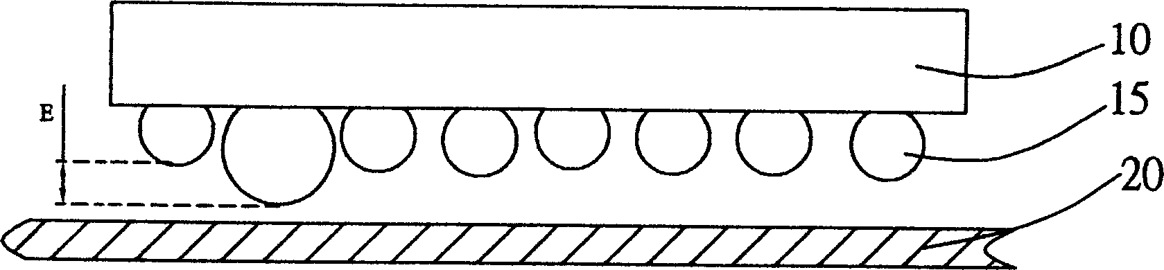
2) if image 3 As shown, assuming that the lower surface 15 of the electrical connector 10 has no bending deformation, when the height difference between the highest soldering leg and the lowest soldering leg is used to measure, the height difference between the highest soldering leg and the lowest soldering leg is E, which may not exceed The theoretical value that guarantees that all soldering feet and the circuit board can be welded by theoretical calculation will judge the product to be qualified
But when the electrical connector 10 is installed on the circuit board 20 (such as Figure 4 As shown), due to the supporting effect of the highest soldering pin, the electrical connector 10 will have a certain
angle of inclination, so the height difference between the lowest soldering pin and the highest soldering pin will be F, which may be greater than the theoretical difference and make the The lowest solder pin cannot make contact with the board

