NFC antenna module and portable terminal having the same
a portable terminal and antenna module technology, applied in the field of nfc antenna modules and portable terminals having the same, can solve the problems of user difficulty in keeping the portable terminal in his or her pocket, the portable terminal is uncomfortable to hold, store, handle, etc., and the height and size of the portable terminal has also become larger. , to achieve the effect of minimizing height and size, increasing the recognition distance thereof, and enlarging the radiation area
- Summary
- Abstract
- Description
- Claims
- Application Information
AI Technical Summary
Benefits of technology
Problems solved by technology
Method used
Image
Examples
first embodiment
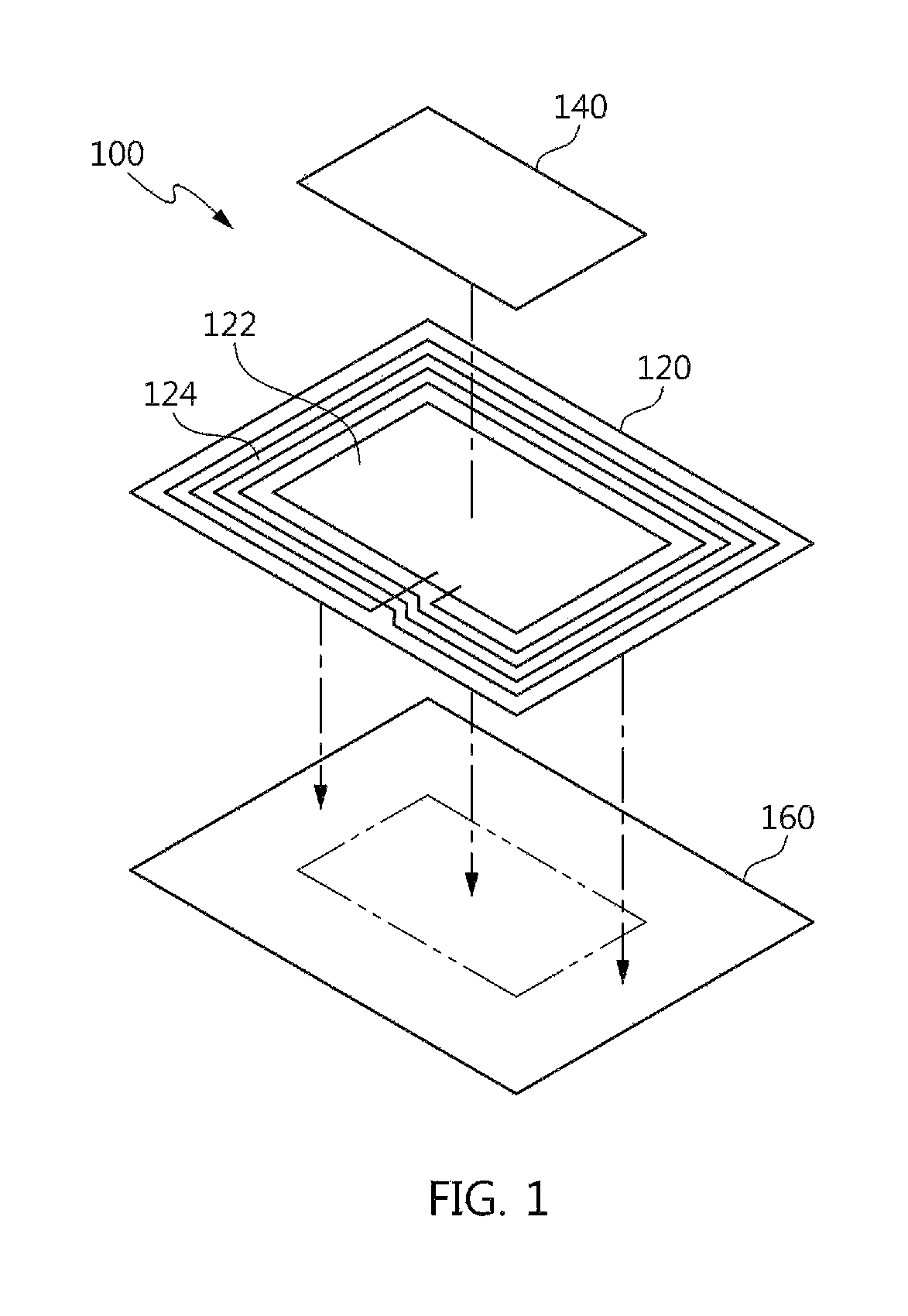
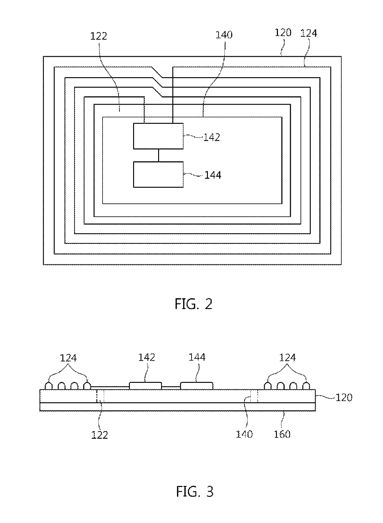
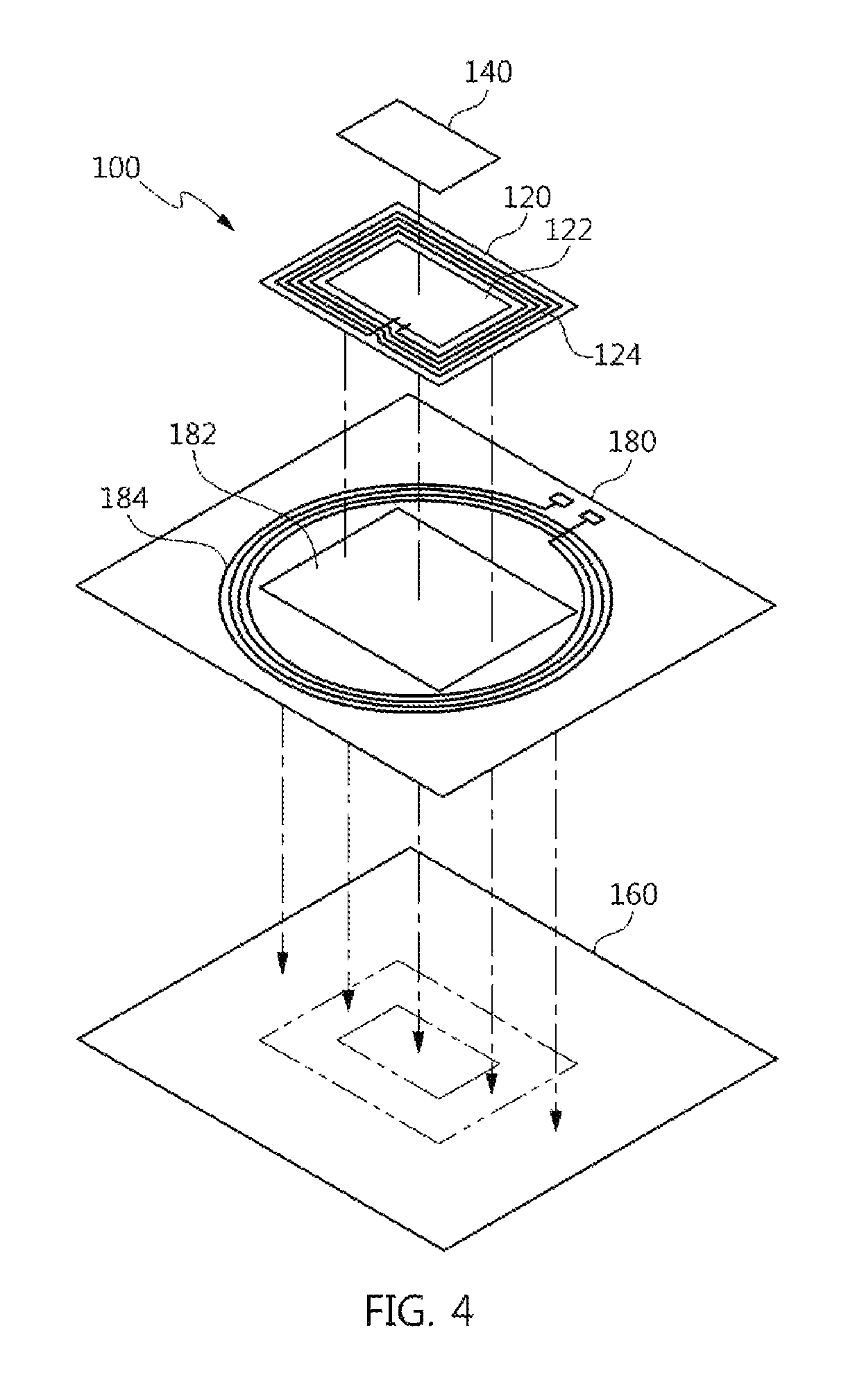
[0034]FIGS. 1 to 4 are views showing an NFC antenna module according to the present invention. The NFC antenna module 100 is included in a wearable terminal such as a smart watch that is produced in a small size to fit on a body, and in a portable terminal such a smartphone, etc. For this, as shown in FIG. 1, the NFC antenna module 100 includes a printed circuit board 140, a first radiation sheet 120, and an electromagnetic wave shielding sheet 160.
[0035]The first radiation sheet 120 is configured with a flexible printed circuit board (FPCB) and includes a first insertion hole 122 into which the printed circuit board 140 is inserted. In other words, the first radiation sheet 120 includes the first insertion hole 122 therethrough that has the same size as or larger than the printed circuit board 140. Herein, the first insertion hole 122 is formed to have the same shape as the printed circuit board 140 (for example, square, rectangle, polygon, etc.)
[0036]The first radiation sheet 120 ...
second embodiment
[0046]FIGS. 6 to 10 are views showing an NFC antenna module according to the present invention. As shown in FIG. 6, the NFC antenna module 300 is configured with a printed circuit board 320, a first radiation sheet 340, and an electromagnetic wave shielding sheet 360.
[0047]The printed circuit board 320 includes an amplification element 322 connected to both ends of a first radiation pattern 344 that is formed on the first radiation sheet 340, and a signal processing element 324. The amplification element 322 and the signal processing element 324 are formed on one surface of the printed circuit board 320. Herein, the amplification element 322 is connected to both ends of the first radiation pattern 344 and amplifies a signal received from the first radiation pattern 344 and transmits the amplified signal to the signal processing element 324. The signal processing element 344 processes the amplified signal and transmits the processed signal to an internal circuit of a portable termina...
PUM
 Abstract
Description
Claims
Application Information


