Look up table including magnetic element, FPGA including the look up table, and technology mapping method of the FPGA

a look-up table and magnetic element technology, applied in the field of look-up tables, can solve the problems of destroying data stored in the sram, requiring a new program to be executed, and requiring a large power consumption, and achieving the effect of reducing the power consumption of the sense amplifier

Active Publication Date: 2019-09-17
SK HYNIX INC +1
View PDF9 Cites 27 Cited by
  • Summary
  • Abstract
  • Description
  • Claims
  • Application Information

AI Technical Summary

Problems solved by technology

Such a conventional LUT is easy to implement a combinational logic circuit and a sequential logic circuit, but when the power is interrupted, data stored in the SRAMs are destroyed and a program must be newly executed.
In addition, an operation speed of the sense amplifier 30 operating in a current mode is relatively slow.
The magnetic circuit 60 selected in FIG. 2 problematically demands a large power consumption because a current must be continuously supplied for the signal output.

Method used


Image

  • Look up table including magnetic element, FPGA including the look up table, and technology mapping method of the FPGA
  • Look up table including magnetic element, FPGA including the look up table, and technology mapping method of the FPGA
  • Look up table including magnetic element, FPGA including the look up table, and technology mapping method of the FPGA

Examples


first embodiment

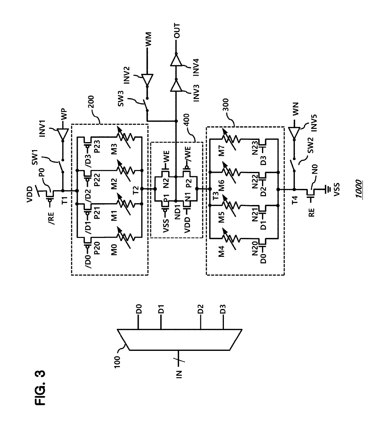
[0046]FIG. 3 illustrates an LUT circuit 1000 according to the present disclosure.

[0047]In this embodiment, the LUT circuit 1000 is for decoding a 2-bit input signal IN. An LUT circuit corresponding to an input signal of a different number of bits will be easily derived from the present disclosure by an ordinary skill in the art.

[0048]The LUT circuit 1000 includes a decoder 100, a first storage unit 200, a second storage unit 300, and a signal input / output (TO) unit 400.

[0049]In this embodiment, the decoder 100 receives the 2-bit input signal IN and outputs four decoded signals D0, D1, D2, and D3. At this time, only one of the four decoded signals D0, D1, D2, and D3 is activated, and the others are deactivated.

[0050]The first storage unit 200 includes a first terminal T1 and a second terminal T2, and includes a plurality of pairs of MTJ cells and switching transistors between the first terminal T1 and the second terminal T2. Each pair includes one MTJ cell and one switching transisto...

second embodiment

[0098]FIG. 4 illustrates a LUT circuit 2000 according to the present disclosure.

[0099]The second embodiment of FIG. 4 differs from the first embodiment of FIG. 3 in that the LUT circuit 2000 further includes a signal input / output (IO) control unit 500.

[0100]In FIG. 3, the power supply voltage VDD is applied to the gate of the first PMOS transistor P1 of the signal IO unit 400, and the ground voltage VSS is applied to the gate of the first NMOS transistor N1 of the signal IO unit 400.

[0101]In FIG. 4, gate voltages of a first PMOS transistor P1 and a first NMOS transistor N1 of a signal IO unit 400-1 are controlled by the signal IO control unit 500.

[0102]In this embodiment, the signal IO control unit 500 controls the gate voltages of the first PMOS transistor P1 and the first NMOS transistor N1 according to a clock signal CLK, a write enable signal WE, and an output signal OUT.

[0103]A first clock signal CLKP and a second clock signal CLKN are generated based on the clock signal CLK an...

third embodiment

[0120]FIG. 5 illustrates a LUT circuit 3000 according to the present disclosure. In FIG. 5, it is possible to implement a LUT circuit that outputs a signal corresponding to the input signal IN when the clock signal CLK is at the low level by applying an inverted clock signal / CLK, rather than the clock signal CLK, to an OR gate 510-1 and an NOR gate 520-1 in a signal IO control unit 500-1.

[0121]The LUT circuit 3000 in FIG. 5 is substantially the same as the LUT circuit 2000 in FIG. 4, except that the inverted clock signal / CLK, which is inverted from the clock signal CLK, is applied to the signal I0 control unit 500-1. The signal IO control circuit 500-1 has substantially the same configuration as the signal IO control circuit 500 shown in FIG. 4.

[0122]Hereinafter, the LUT circuit 1000 shown in FIG. 3 can be referred to as a first LUT circuit 1000, the LUT circuit 2000 shown in FIG. 4 as a second LUT circuit, and the LUT circuit 3000 shown in FIG. 5 as a third LUT circuit.

[0123]Gene...


PUM


Abstract

A look up table (LUT) includes a decoder configured to decode input signals and to output decoded signals, a storage unit including a plurality of magnetic elements an being configured to select one or more of the plurality of magnetic elements in response to the decoded signals and a signal input / output (TO) unit configured to output an output signal corresponding to the selected one or more magnetic elements and to program the selected one or more magnetic elements by receiving a write signal.

Description

CROSS-REFERENCE TO RELATED APPLICATION[0001]The present application claims priority to Korean Patent Application No. 10-2017-0038994, filed on Mar. 28, 2017, which is incorporated by reference herein in its entirety.BACKGROUND1. Field[0002]Embodiments of the present disclosure relate to a Look Up Table (LUT) including a magnetic element, a Field Programmable Gate Array (FPGA) including the LUT, and a technology mapping method applicable to the FPGA.[0003]More particularly, embodiments of the present disclosure relate to a LUT capable of reducing a cell area and a static current, an FPGA including the LUT, and a technology mapping method applicable to the FPGA.2. Description of the Related Art[0004]A Field Programmable Gate Array (FPGA) is a type of Programmable Logic Device (PLD) that is widely used to design digital circuits that perform specific operations through programs.[0005]The FPGA includes configurable logic blocks (CLBs), input / output blocks (IOBs), and configurable connec...

Claims


Application Information

Patent Timeline
Patent Type & Authority Patents(United States)
IPC IPC(8): G06F17/50H03K19/00H03K19/177H03K19/173H03K19/20G11C11/16
CPCH03K19/0013H03K19/1731G06F17/5054H03K19/1776H03K19/17744G06F17/505H03K19/20G11C11/1673G11C11/1675G06F30/34G11C11/1653H03K19/17728G06F30/327
Inventor JO, KANGWOOKKIM, JEONGBINIM, MINYOUNGYOU, TAEHEECHUNG, EUI-YOUNGYOON, HONGIL
Owner SK HYNIX INC
Why Eureka
Try Eureka