
Label free analyte detection by electronic desalting and field effect transistors

a field effect transistor and label detection technology, applied in the field of label free sensing, can solve the problems of sample preparation, certain limitations of fet sensing, and the common disadvantage of conventional sensing systems, and achieve the effects of improving sensor response and detection characteristics, facilitating label free analyte sensing, and high ionic strength

Active Publication Date: 2020-01-07
THE BOARD OF TRUSTEES OF THE UNIV OF ILLINOIS
View PDF25 Cites 1 Cited by
  • Summary
  • Abstract
  • Description
  • Claims
  • Application Information

AI Technical Summary

Benefits of technology

[0011]Provided herein are methods and related devices for label free sensing using FETs having improved sensor response and detection characteristics. In particular, the special geometry of the systems provided herein, including locally patterned on-chip metal electrodes in close proximity to the FET, allow for simultaneous electrical desalting and FET gating and corresponding analyte sensing. Other aspects that facilitate label free analyte sensing in high ionic strength solutions include reduced sample volume, such as in a droplet and also increased in effective surface area of the reference electrodes.
[0012]Conventional FET systems comprise a transistor whose gate is exposed to an ionic medium, with a gate voltage that determines conduction that is applied by a fluidic standard reference electrode. Sensing is then accomplished by an analyte reaction that affects change in the concentration of an ion or pH, which in turn perturbs the gate voltage. Detection of a change in the gate voltage provides an indication of analyte. In the methods and systems provided herein, the fluidic reference electrode is replaced by on-chip reference electrodes in close proximity to the FET. The reference electrodes may be precisely positioned and have precise geometrical layout, such as by patterning methods known in the art, including lithography and other microfabrication methods. In an aspect, the reference electrodes are arranged in a paired geometry, with the electrodes opposibly configured to one another and the sensor of the FET disposed therebetween in close proximity. In any of the methods and devices provided herein, the reference electrodes in this geometry are energized so as to attract charged carriers, such as ions, dissolved salts and electrolytes from the FET sensor to the surface of the reference electrodes, thereby reducing the screening effects associated with the charged ions. Both negatively and positively charged ions are attracted to a reference electrode by energizing one of the reference electrodes with a positive electric potential and the counter-electrode with a negative electric potential.
[0013]In an aspect, the potentials are selected so as to also provide an appropriate gate voltage to the FET. In this manner, the conventional fluidic standard reference electrode is replaced with the reference electrodes provided herein and the gate voltage may be described as coupled to the reference electrodes that are also electrically desalting the sample solution. Any of the methods provided herein relate to use of small sample volumes so that the electrodes can attract charged ions from throughout the sample, thereby avoiding a tendency of charged ions to simply backfill the depleted ion region from the rest of the sample solution via diffusion. In this manner, the fluid droplet is preferentially flattened and covers a significant portion or all the reference electrode contact surface area. Accordingly, any of the methods provided herein relate to electrode contact surface area having an increased working contact surface area, such as by processing the surface to increase surface area via roughening, or through the use of porous electrodes that increase surface area available to interact with charged ions.

Problems solved by technology

Such conventional sensing systems suffer a common disadvantage of requiring sample preparation, such as one or more of washing, isolation, incubation, temperature control and other handling dependent on the biosensor type.
There are, however, certain limitations associated with FET sensing, particularly as applied to biological applications.

Method used


Image

  • Label free analyte detection by electronic desalting and field effect transistors
  • Label free analyte detection by electronic desalting and field effect transistors
  • Label free analyte detection by electronic desalting and field effect transistors

Examples


example 1

References for Example 1

[0149]1. P. Bergveld, “Thirty years of ISFETOLOGY, What happened in the past 30 years and what may happen in the next 30 years,”Sensors and Actuators B: Chemical 88 (2003): 1-20.[0150]2. P. Bergveld, “The development and application of FET-based biosensors.”Biosensors 2(1) (1986): 15-33.[0151]3. A. van den Berg et al., “A micro-volume open liquid-junction reference electrode for pH-ISFETs.”Sensors and Actuators B: Chemical 1 (1990): 425-432.[0152]4. J. M. Rothberg et al., “An integrated semiconductor device enabling non-optical genome sequencing,”Nature, 475 (2011): 348-352.[0153]5. W. Guan et al., “Field-effect reconfigurable nanofluidic ionic diodes,”Nature Communications, 2 (2011): 506.[0154]6. B. R. Dorvel et al., “Fabrication of High-k Hafnium Oxide Based Silicon Nanowires for Sensitive Detection of Small Nucleic Acid Oligomers,”ACS Nano, 6(7) (2012): 6150-6164.[0155]7. J. Go et al., “Coupled Heterogeneous ‘Nanowire-Nanoplate’ Planar Transistor Sensors f...

example 2

Characterization of NanoFETs with On-chip Platinum Electrodes

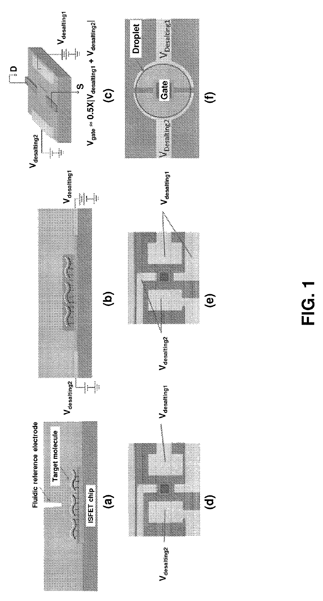
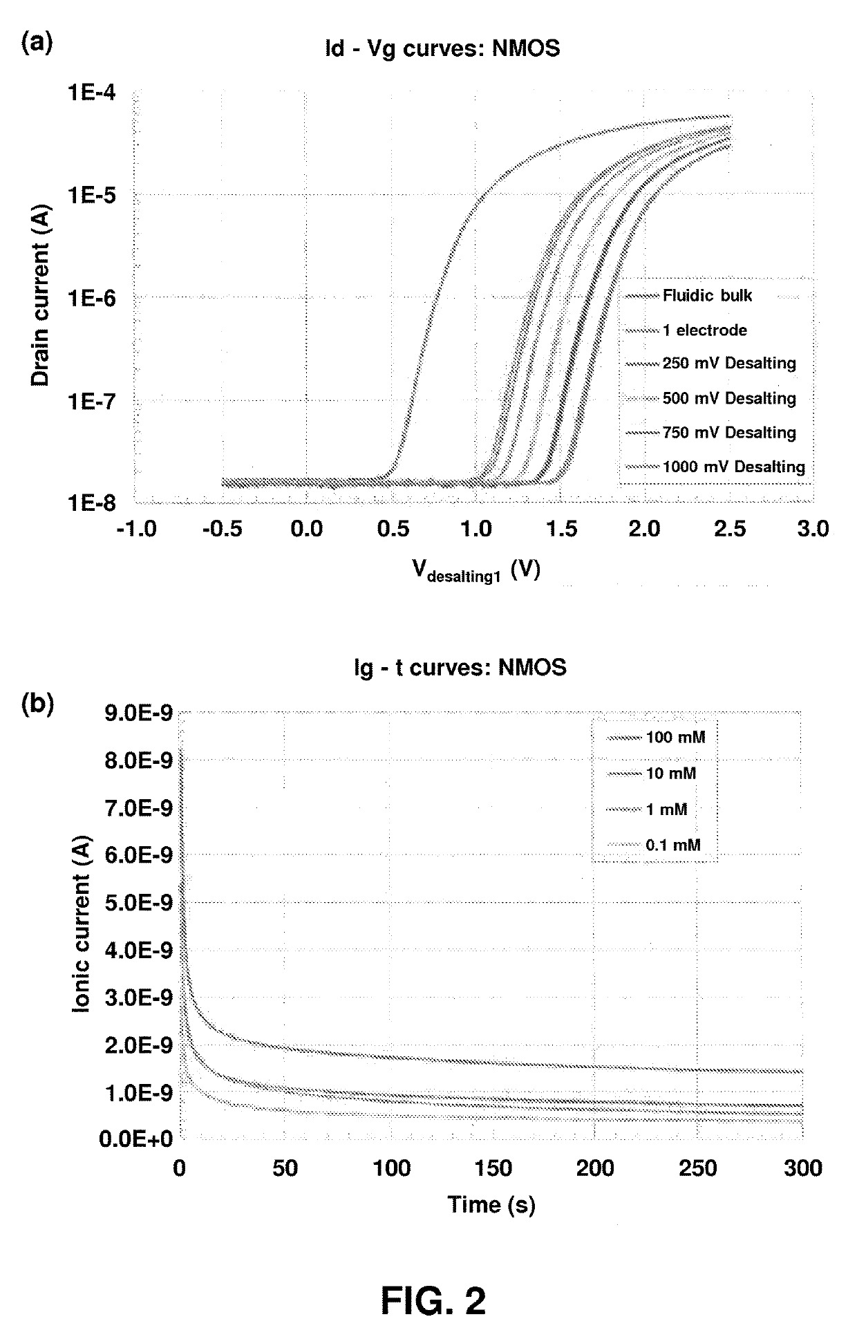
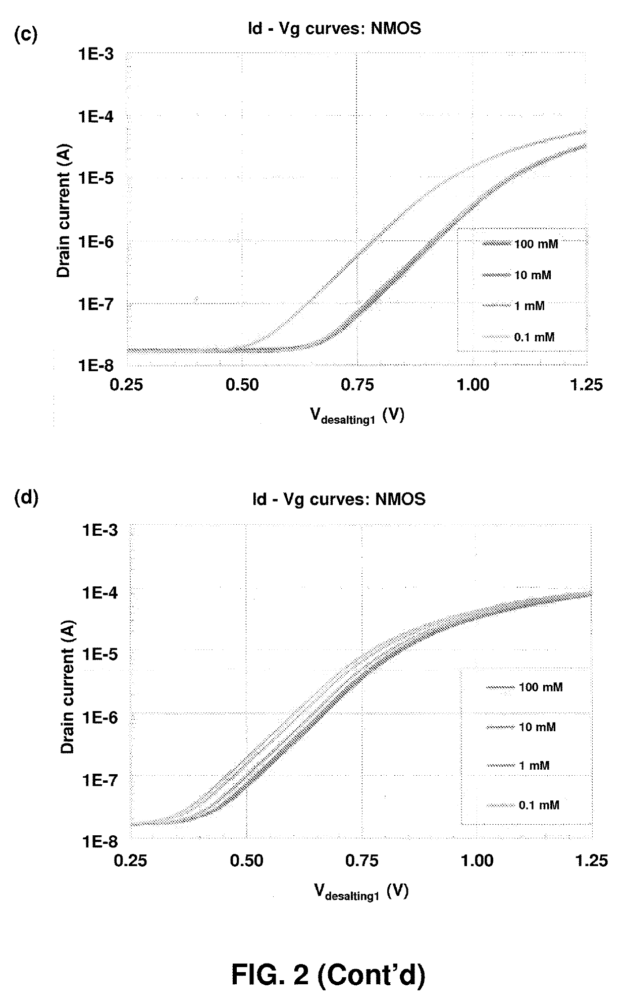
[0160]NanoFETs and on-chip platinum electrodes are examined to further explore and characterize device and biasing schematics. Dye visualization is employed to examine desalting around the devices, including MQAE (Cl−) and SNARF-5F (pH) dyes (see FIG. 5). Further explored are multiple pairs of reference electrodes that surround the FET. To characterize biasing conditions, one electrode is swept while the second electrode of the pair is grounded; and both reference electrodes are swept with an offset. The biasing experiments indicate a fixed desalting voltage with respect to the gate voltage is more stable. This can eliminate interference associated with FET on / off behavior and also eliminates Faradaic overpotential when at large gate voltages.

[0161]Referring to FIG. 5, dyes are attached to aminosilanized surface using EDC-NHS leaving group chemistry. Ester hydrolysis to carboxylic acid preserves fluorophores for MQAE dye. ...

example 3

Paired Electrodes Around Gate

[0168]FIGS. 17-18 illustrate an increase in metal electrode surface area by more than a factor of 2 to capture more ions. Furthermore, this configuration helps anchor the droplet by wetting of the metal surface around the FET sensor gate. FIGS. 17-18 show a substrate 100, such as a chip, supporting a FET 200, including FET sensor 210, source 230, drain 240, and patterned reference electrodes 310 and 320. Sensor 210 is illustrated as a nanowire with corresponding sensor area 220. Reference electrodes 310 and 320 are paired and opposibly face each other separated by a separation distance 330. Electrical controllers 410 and 420 are electrically connected to reference electrodes. Fluid sample is positioned within a well 500 so as to substantially cover the working surface area of reference electrodes 310 and 320 (e.g., the semi-circular shaped portion). Electrical sensor 600 and / or 610 are connected to the FET to monitor an electrical parameter, wherein a ch...


PUM

PropertyMeasurementUnit
Debye screening lengthaaaaaaaaaa
ionic strengthaaaaaaaaaa

Abstract

Provided are methods and devices for the label free detection of analytes in solution, including analytes suspended in a biological fluid. A field effect transistor (FET) is positioned in close proximity to a paired set of reference electrodes and the reference electrodes electrically biased to provide desalting and a stable gate voltage to the FET. In this manner, charged ions are depleted in the sensing region of the sensor and device sensitivity to analyte detection improved by the removal of charge that otherwise interferes with measurement. Also provided are methods and systems providing increased in reference electrode surface area and / or decrease in droplet volume to further improve label-free detection of analytes.

Description

CROSS-REFERENCE TO RELATED APPLICATIONS[0001]This application claims the benefit of priority to U.S. Provisional Patent Application Nos. 62 / 007,808 filed on Jun. 4, 2014, and 61 / 972,148 filed Mar. 28, 2014, each of which is specifically incorporated by reference to the extent not inconsistent herewith.STATEMENT REGARDING FEDERALLY SPONSORED RESEARCH OR DEVELOPMENT[0002]This invention was made with government support under R01CA120003 awarded by the National Institutes of Health, and EEC-0425626 awarded by the National Science Foundation. The government has certain rights in the invention.BACKGROUND OF INVENTION[0003]The invention is in the field of label free sensing, including label free electronic biomolecular detection using field effect transistors, including ion-sensitive-field-effect-transistors. The invention generally relates to methods for analyte detection and associated devices, particularly analytes comprising biological material suspended in biological material compatib...

Claims


Application Information

Patent Timeline
Patent Type & Authority Patents(United States)
IPC IPC(8): G01N27/414G01N33/543
CPCG01N27/4146G01N27/4145G01N33/5438
Inventor BASHIR, RASHIDVILASUR SWAMINATHAN, VIKHRAMREDDY, JR., BOBBYSALM, ERIC M.DUARTE-GUEVARA, CARLOS
Owner THE BOARD OF TRUSTEES OF THE UNIV OF ILLINOIS
Learn More