SOI active pixel cell design with grounded body contact

a technology of active pixel and body contact, which is applied in the direction of semiconductor devices, electrical equipment, radio frequency controlled devices, etc., can solve the problems of excess electron spilling out and disturbing adjacent aps cells, overexposed aps pixels can interfere with the proper operation of other devices on the substrate, and the charge that can be collected and held in the pin diode is limited

Inactive Publication Date: 2001-09-27
GLOBALFOUNDRIES INC
View PDF0 Cites 25 Cited by
  • Summary
  • Abstract
  • Description
  • Claims
  • Application Information

AI Technical Summary

Benefits of technology

0023] Regardless of whether the filled trench design or the individual vertical plug design is used to make the body to pinning layer connection, it is generally desirable to connect these elements to ground and to the corresponding elements of the other pixel cells. This may be achieved simply by individually connecting wires to each cell when wi...

Problems solved by technology

One difficulty with APS designs is that the amount of charge that can be collected and held in the pin diode is limited by the total reverse potential of the diode.
Excess electrons will then spill out and disturb adjacent APS cells.
The excess electrons from overexposed APS pixels can also interfere with...

Method used


Image

  • SOI active pixel cell design with grounded body contact
  • SOI active pixel cell design with grounded body contact
  • SOI active pixel cell design with grounded body contact

Examples


Embodiment Construction

)

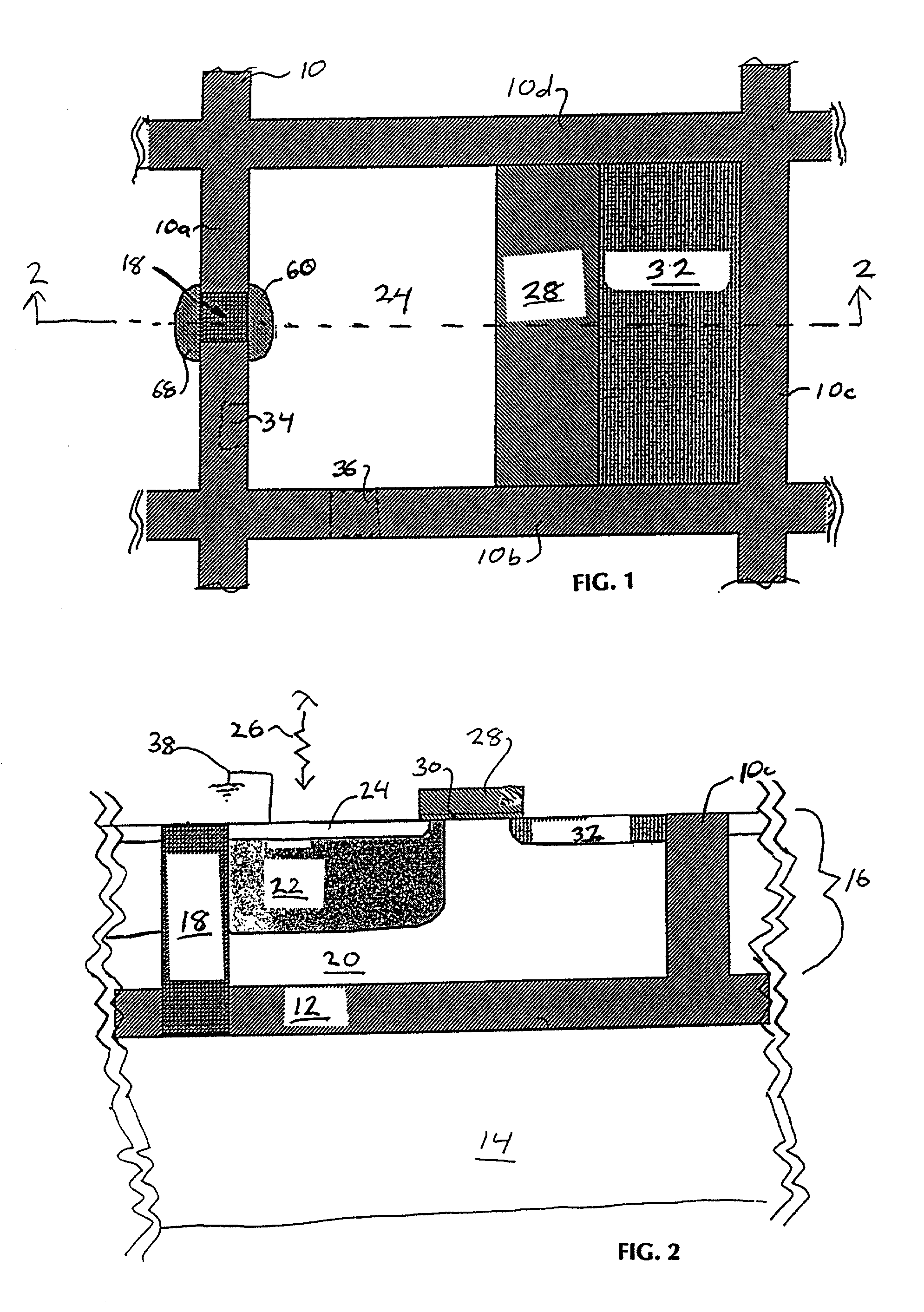
[0042] In describing the preferred embodiment of the present invention, reference will be made herein to FIGS. 1-11 of the drawings in which like numerals refer to like features of the invention.

[0043] FIGS. 1 and 2 illustrate a first embodiment of the photosensitive device of the present invention. In this embodiment, each APS device has a separate semiconductor plug in the form of a vertical column of semiconductor material to connect the body of the APS device to its pinning layer.

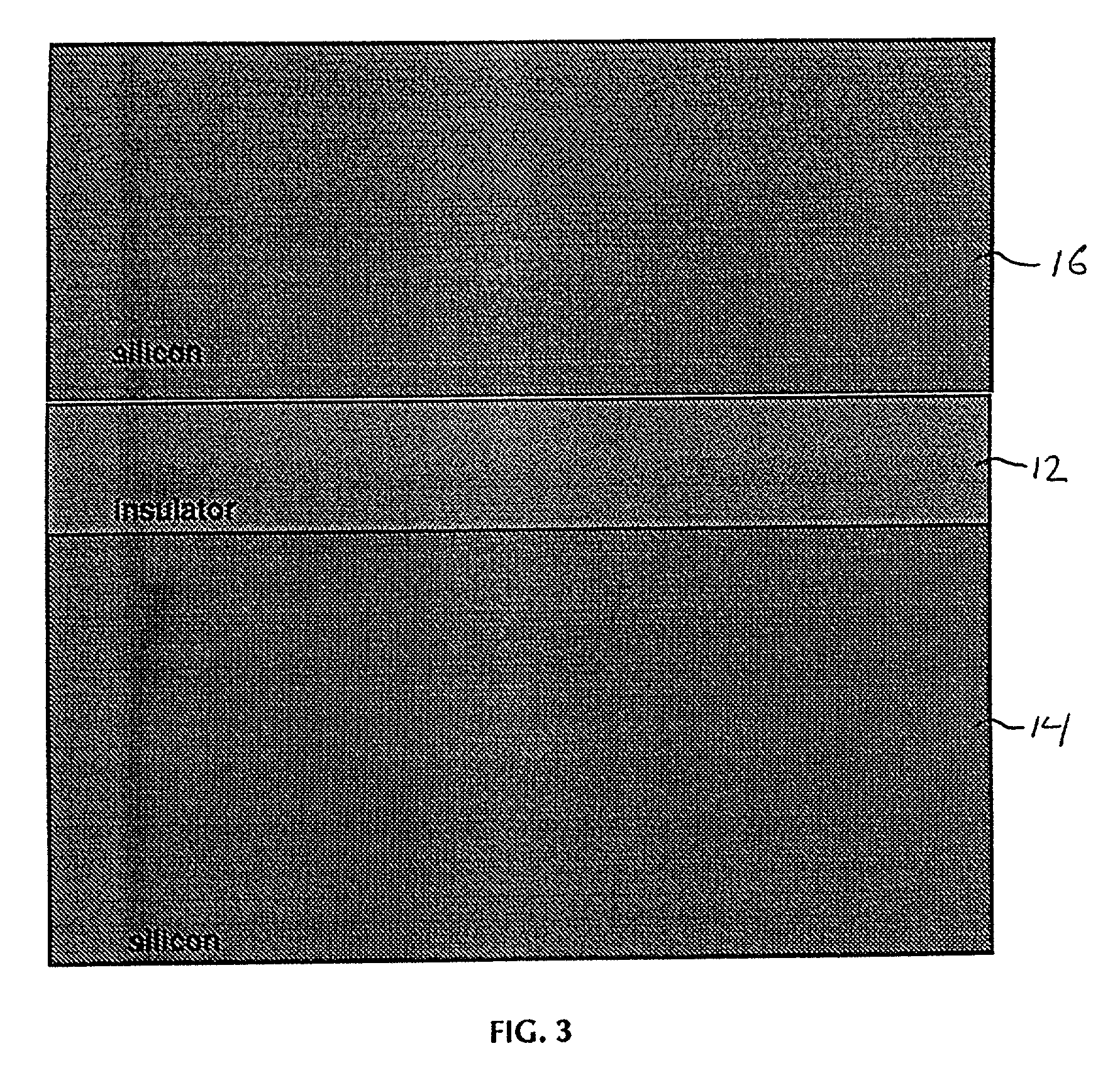
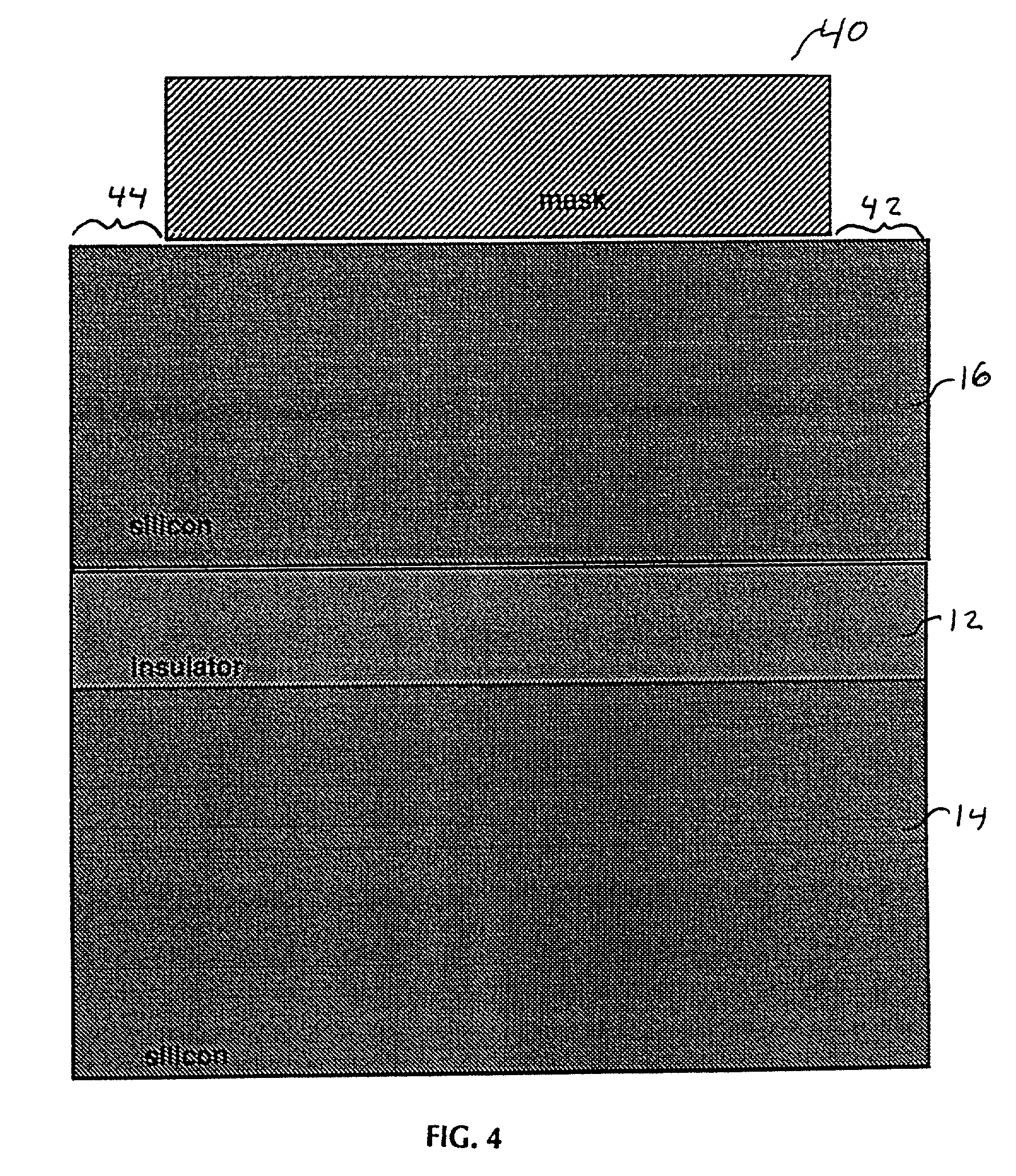
[0044] The present invention comprises a photosensitive device incorporating an array of active pixel sensors devices, each APS device being constructed in an isolated island of silicon surrounded on all sides by a barrier of insulating material, and isolated below by an insulating layer. FIG. 1 provides a top plan view showing a single cell in the array. The cell is surrounded on four sides by insulating barrier 10, the portions of the insulating material surrounding the sides being indicated with ref...


PUM


Abstract

A photosensitive device includes an array of active pixel sensor devices, each APS device being formed in an isolated cell of silicon. Each cell has an insulating barrier around it, and sits upon an insulating layer formed on an underlying substrate. A semiconductor connector making vertical contact between the pinning layer and the body of each APS device preferably replaces at least some portion of the insulating barrier adjacent to each cell. The semiconductor connector may be a single vertical connection for each cell or it may be an elongated strip connecting multiple APS devices. It may extend only to the underlying insulating layer or it may extend through the insulating layer to the substrate, with the substrate acting to interconnect and ground the pinning layer and the body of each APS device. The invention also includes the method of making the photosensitive device.

Description

[0001] 1. Field of the Invention[0002] This invention relates to solid state image sensors, and more particularly, to active pixel sensor (APS) technology.[0003] 2. Description of Related Art[0004] Active pixel sensors and charge coupled devices (CCD) are solid state photosensitive devices which are commonly constructed as an array of photosensitive cells, each cell in the array corresponding to a pixel. A typical application for CCD or APS image sensing arrays is in a digital camera or other type of image sensor.[0005] One advantage to APS devices over CCD devices is that APS technology is more compatible with metal oxide semiconductor (MOS) technology. This allows the support electronics needed to read signals from the APS array, and to process those signals, to be constructed on the same chip and at the same time as the APS array itself. This can significantly reduce the total cost of an APS technology based imaging device.[0006] A basic prior art APS device comprises a reverse-b...

Claims


Application Information

Patent Timeline
IPC IPC(8): H01L27/146
CPCH01L27/14609H01L27/1463
Inventor JOHNSON, JEFFREY B.WONG, HON-SUM P.
Owner GLOBALFOUNDRIES INC
Why Eureka
Try Eureka