Technique for flagging oversaturated pixels

a technology of oversaturated pixels and flagging, which is applied in the field of digital imaging sensors, can solve the problems of slow readout rate, large power requirements, and inability to integrate on-chip signal processing electronics in ccd imagers, and achieve the effects of reducing the cost of ccd imagers, and improving the accuracy of ccd imagers

Inactive Publication Date: 2005-03-29
APTINA IMAGING CORP
View PDF9 Cites 63 Cited by
  • Summary
  • Abstract
  • Description
  • Claims
  • Application Information

AI Technical Summary

Benefits of technology

[0013]FIG. 1 illustrates such a situation in a digital image 10 produced using a conventional APS CMOS imag...

Problems solved by technology

However, the standard CCD formation process often is incompatible with CMOS processing.
Accordingly, it is impractical to integrate on-chip signal processing electronics in a CCD imager and the signal processing electronics must be provided off-chip.
This operation requires nearly perfect charge transfer efficiency, resulting in slow readout rates and relatively large power requirements.
Conve...

Method used


Image

  • Technique for flagging oversaturated pixels
  • Technique for flagging oversaturated pixels
  • Technique for flagging oversaturated pixels

Examples


Embodiment Construction

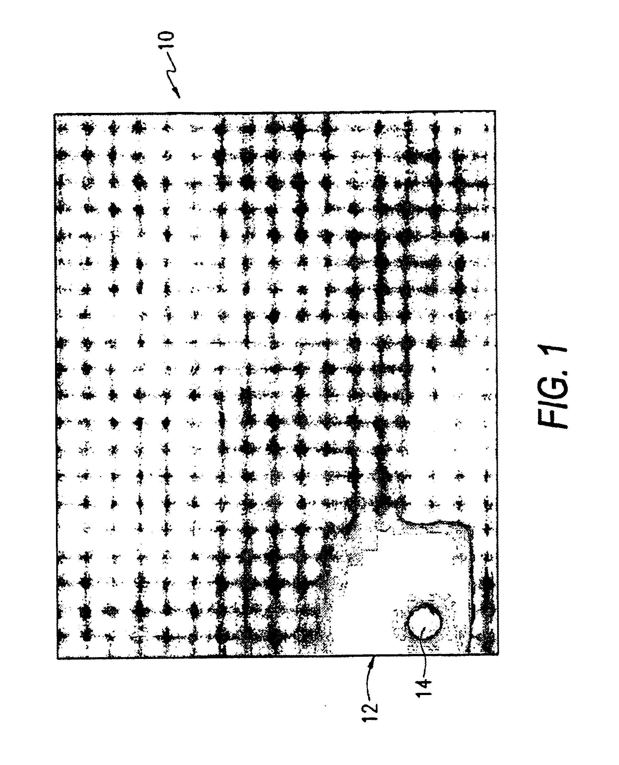
mage including an artifact produced in the center of the sun caused by oversaturated pixels.

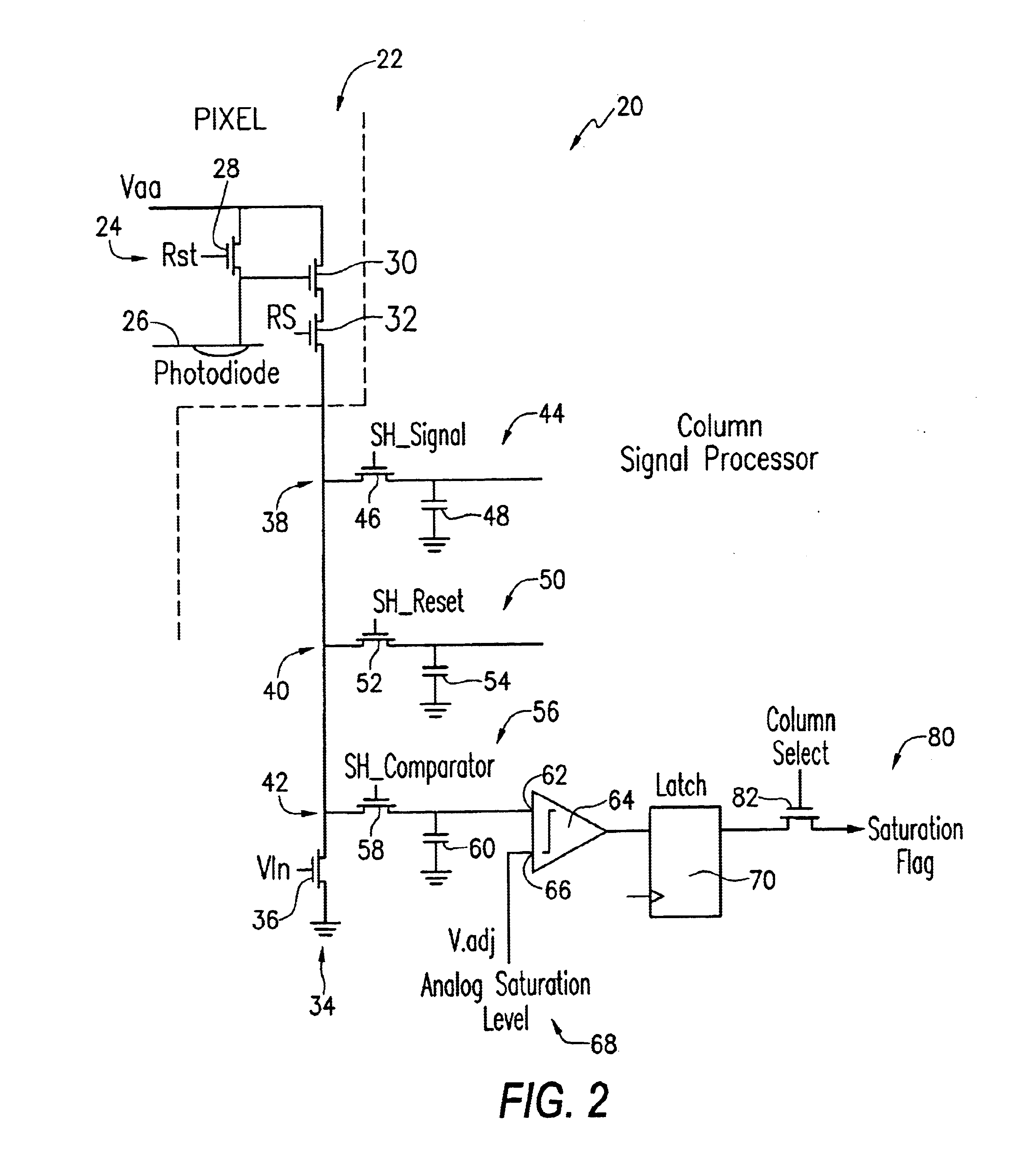
[0019]FIG. 2 is a schematic diagram according to an embodiment of the invention.

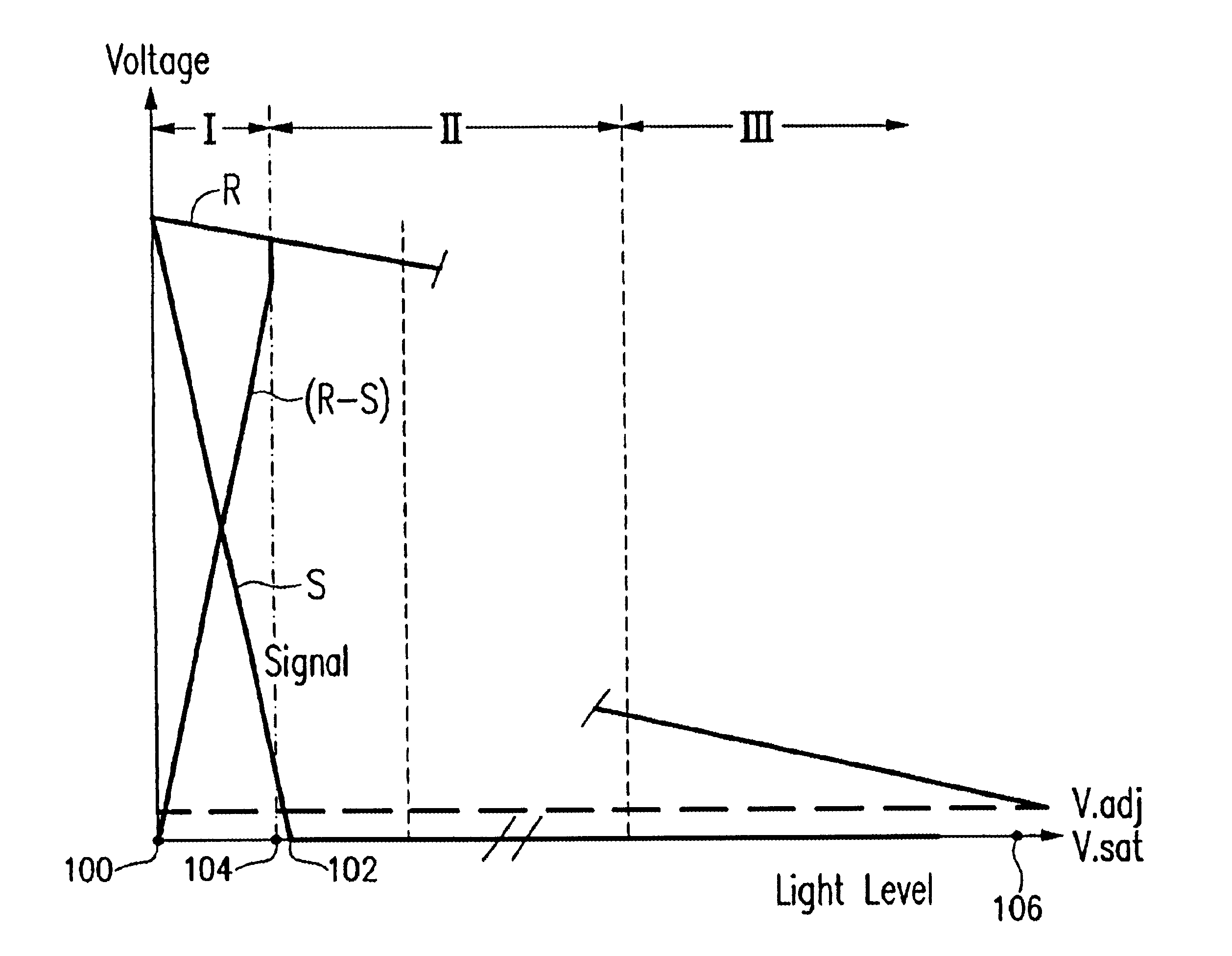
[0020]FIG. 3 is a chart showing the response of voltage levels to incident light levels according to the embodiment of FIG. 2.

[0021]FIG. 4 is a schematic diagram showing another embodiment of the invention including digital processing circuitry.

[0022]FIG. 5 is a schematic diagram showing another embodiment of the invention in which the APS has a column-parallel architecture.

[0023]Like reference symbols in the various drawings indicate like elements.

DETAILED DESCRIPTION

[0024]Oversaturated pixels in an active pixel sensor (APS) imaging device can produce artifacts in the resulting images in high contrast situations. Artifacts are objects in the image that appear black, but in fact should be the brightest objects in the image.

[0025]According to the present embodiment, oversaturated pixels in an APS pixel array are fl...


PUM


Abstract

An active pixel sensor (APS) that includes circuitry to eliminate artifacts in digital images. The APS includes a comparator for comparing a signal level from a pixel to an adjusted saturation voltage to determine if the pixel is saturated. If the pixel is saturated, an associated saturation flag is stored and used to replace the signal from the pixel with a maximum value corresponding to a brightest pixel in the image.

Description

CROSS REFERENCE TO RELATED APPLICATION[0002]This application claims the benefit of the U.S. Provisional Application No. 60 / 120,423 entitled TECHNIQUE FOR FLAGGING OVERSATURATED PIXELS filed on Feb. 16, 1999.TECHNICAL FIELD[0003]This invention relates to digital imaging sensors, and more particularly to active-pixel sensors.BACKGROUND[0004]Charge coupled devices (CCD) have traditionally been the imagers of choice for high quality imaging devices due to their high sensitivity and fill-factor. However, the standard CCD formation process often is incompatible with CMOS processing. Accordingly, it is impractical to integrate on-chip signal processing electronics in a CCD imager and the signal processing electronics must be provided off-chip.[0005]CCDs are essentially electronic analog shift registers. CCDs include rows of photodetectors that act essentially as capacitors. Each pixel converts light energy into a charge, and then transfers that charge sequentially across a row of pixels in...

Claims


Application Information

Patent Timeline
IPC IPC(8): H04N3/14H04N5/335H04N5/367H04N5/374H04N5/378
CPCH04N5/378H04N5/3598H04N25/627H04N25/75
Inventor BARNA, SANDOR L.FOSSUM, ERIC R.
Owner APTINA IMAGING CORP
Why Eureka
Try Eureka