Method and circuit for performing correlated double sub-sampling (CDSS) of pixels in an active pixel sensor (APS) array

a technology of active pixel sensor and subsampling method, which is applied in the field of image sensors, can solve the problems of ccd sensor, comparatively high energy consumption, and inability to sustain high-speed operation, and achieve the effect of reducing the error rate of the output signal, reducing the efficiency of the aps, and reducing the aps

Active Publication Date: 2005-09-22
SAMSUNG ELECTRONICS CO LTD
View PDF18 Cites 63 Cited by
  • Summary
  • Abstract
  • Description
  • Claims
  • Application Information

AI Technical Summary

Benefits of technology

[0025] It follows from this mathematical relationship that the precise “average” value of four CDS-sampled pixel values to be averaged together (subsampled) can be obtained by (analog) subtraction of a combination of the four “reset” charges (QR11+QR13+QR31+QR33 of the four pixels) from a combination of the four “signal” charges QS11+QS13+QS31+QS33 of the four pixels. The combination of the four “signal” charges can be “divided” by four (e.g., prior to “subtracting” the combined “reset” charge) by distributing that combined charge (e.g., equally) between four capacitors of equal capacitance (e.g., C). Similarly, the combination of the four “reset” charges can then be “divided” by four (e.g., prior to “subtraction” from the combined “signal” charges) by distributing that combined charge (e.g., equally) between four capacitors of equal capacitance (e.g., C). Thus, the “average” value of four CDS-sampled pixels can be obtained by performing the steps of: combining and dividing (averaging, sub-sampling) the four associated “reset” charges to obtain an averaged reset charge QRAVG; combining and dividing (averaging, subsampling) the four associated “signal” charges to obtain an averaged signal charge QSAVG; and then performing one correlated double sampling operation (a subtraction) by subtracting the averaged reset charge QRAVG from the averaged signal charge QSAVG. This general method is herein referred to as correlated double sub-sampling (CDSS) because the result of the method is a precisely sub...

Problems solved by technology

While, the charge coupled device CCD was virtually the principal image pickup device, the core of digital cameras, the CCD sensor is disadvantageous in that it consumes comparatively high amounts of energy and does not sustain high-speed operation.
Components, such as the switch, due to its finite residual conductivity, can precharge the capacitor to an unknown value, and this adds error to the output signal.
However, it may be difficult in practice to maintain a ...

Method used


Image

  • Method and circuit for performing correlated double sub-sampling (CDSS) of pixels in an active pixel sensor (APS) array
  • Method and circuit for performing correlated double sub-sampling (CDSS) of pixels in an active pixel sensor (APS) array
  • Method and circuit for performing correlated double sub-sampling (CDSS) of pixels in an active pixel sensor (APS) array

Examples


Embodiment Construction

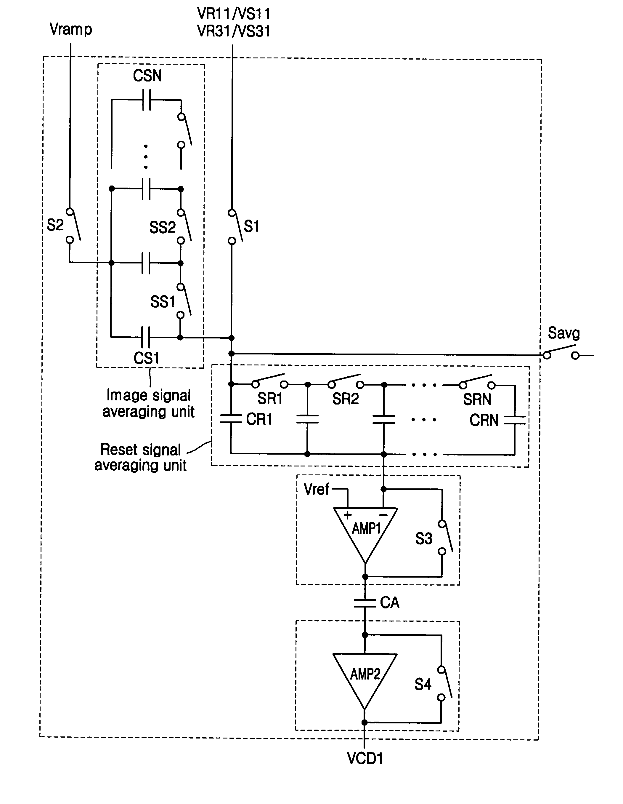
[0041]FIG. 3 is a block diagram illustrating a CMOS image sensor (CIS) unit, including an active pixel sensor (APS) array, and an Averaging & Comparing circuit for performing Correlated Double Sub-Sampling (CDSS), according to an exemplary embodiment of the present invention. FIG. 4 is a circuit diagram illustrating an exemplary structure of each pixel within the active pixel sensor (APS) array of the CIS of FIG. 3.

[0042] Referring to FIG. 3 and FIG. 4, the active pixel sensor (APS) array may be comprised of a plurality of pixel circuits known in the related art, or preferably, the pixel circuit of FIG. 4, adapted to sequentially output a VR(reset) voltage and a VS(image signal) voltage. Each pixel in the APS array will generally include a photo-electric transducer (e.g., photodiode PD of FIG. 4). The Row Driver circuit is generally known in the related art and is adapted here to sequentially select pairs of odd (1,3 . . . ) and then pairs of even (2,4 . . . ) numbered rows during ...


PUM


Abstract

A method and circuit for performing Correlated Double Sub-Sampling (CDSS) of pixels in an active pixel sensor (APS) array. Each pixel outputs a reset voltage and then an image signal voltage. The method and the apparatus subsamples a plurality (L2 ) of pixels by: storing L2 analog reset charges output from the L2 pixels into a first set of (N2) storage capacitors, and combining the (L2) reset charges; storing L2 analog image signal charges output from the L2 pixels into a second set of (N2) storage capacitors, and combining the (L2) image charges; and then obtaining a differential voltage (VS−VR) by subtracting (in the analog-domain) the voltage (VR) represented by the combined (L2) reset charges from the voltage (VS) represented by the combined (L2) image signal charges. When L equals one, the circuit performs conventional Correlated Double Sampling CDS upon the one pixel. When L is greater than one, the circuit performs Correlated Double Sub-Sampling (CDSS) of the L2 pixels. Dynamic selection of a subsampling ratio B (where B equals 1:L2 and L ranges from 1 up to N) is supported. Averaging units used to combine the reset and image signal charges, and analog-to-digital converters (ADCs) for converting the differential voltage to a digital pixel data, may be commonly biased by the same variable bias voltage.

Description

FIELD OF THE INVENTION [0001] The present invention relates to image sensors, more particularly to a method and circuit able to perform Correlated Double Sub-Sampling (sub-sampling and then correlated double sampling (CDS)) of a dynamically selected number of pixels in an N×M pixel region of an active pixel sensor (APS) Array. DISCUSSION OF RELATED ART [0002] Since the mid 1980's, the most common image pickup device (image sensor) has been the charge coupled device (CCD). Backed by the semiconductor industry, CCD capabilities advanced rapidly, eventually resulting in the present small high-performance cameras. While, the charge coupled device CCD was virtually the principal image pickup device, the core of digital cameras, the CCD sensor is disadvantageous in that it consumes comparatively high amounts of energy and does not sustain high-speed operation. In view of this situation, large CMOS image sensors (CIS), which offer a high resolution of multiple megapixels (Mps), have been d...

Claims


Application Information

Patent Timeline
IPC IPC(8): H04N3/15H04N5/335
CPCH04N5/3575H04N5/378H04N5/365H04N25/616H04N25/67H04N25/75H04N25/40
Inventor LIM, SUHUN
Owner SAMSUNG ELECTRONICS CO LTD
Why Eureka
Try Eureka