CMOS sensor with electrodes across photodetectors at approximately equal potential

a technology of photodetectors and electrodes, applied in the field of cmos sensors, can solve the problems of reset clock noise and dark current noise, and cmos active pixel noise, so as to reduce or eliminate dark current, eliminate clock noise, and eliminate clock noise.

Inactive Publication Date: 2009-04-28
E PHOCUS
View PDF1 Cites 67 Cited by
  • Summary
  • Abstract
  • Description
  • Claims
  • Application Information

AI Technical Summary

Benefits of technology

[0025]The present invention provides a MOS or CMOS based active pixel sensor designed for operation with zero or close to zero potential across the pixel photodiodes to minimize or eliminate dark current. In preferred embodiments the pixel photodiodes are produced with a continuous pin or nip photodiode layer laid down over pixel electrodes of the sensor. In this preferred embodiment, the voltage potential across the pixel photodiode structures is maintained constant and close to zero, preferably less than 1.0 volts. This preferred embodiment enables the photodiode to be operated at a constant bias condition during the charge detection cycle. Setting this constant bias condition close to zero (near “short circuit” condition) assures that dark current is substantially zero.
[0026]In other preferred embodiments in addition to minimizing or eliminating dark current with zero or close to zero potential across the pixel photodiodes, the sensor is provided with special sampling features to substantially eliminate clock noise. The sensor includes an array of pixels fabricated in or on a substrate, each pixel defining a charge collection node on which charges generated inside a photodiode region are collected, a charge integration node, at which charges generated in said pixel are integrated to produce pixel signals, a charge sensing node from which reset signals and the pixel signals are sensed. In preferred embodiments the sensor includes a continuous electromagnetic radiation detection structure located above the pixel circuits providing a photodiode region for each pixel. The sensor includes integrated circuit elements adapted to maintain voltage potentials at the charge collection nodes substantially constant during charge integration cycles. The sensor also includes integrated circuit elements having electrical capacitance adapted to store charges providing an electrical potential at the charge integration node. In preferred embodiments this is a pinned diode. The sensor also includes a transfer switch to transfer charges from the charge integration node to the charge sensing node. The sensor also includes integrated circuit elements having electrical capacitance adapted to store charges providing an electrical potential at the charge sensing node. The sensor also includes integrated circuit elements adapted to reset the charge sensing node and the charge integration node, integrated circuit elements adapted to convert the charges on the charge sensing node into electrical signal, and integrated circuit elements adapted to readout electrical signals generated in the pixels.
[0027]One of the very important features of preferred embodiments of this invention is that the charge integration node and charge sensing node are separated from each other. This feature permits correlated double sampling that basically eliminate clock noise as a problem.
[0029]This novel design resolves the concern of incomplete charge transfer on the charges stored on the photodiode (and its associated circuitry) since there is no charge transfer from the photodiode region during the signal readout cycles. This is especially important if the photodiode is on pixel circuitry (like POAP) where the charges stored on the photodiode needs to travel through vias and interlayer metal connectors in order to get to the charge sensing node. This travel path can not be fabricated with perfection in real practice; therefore, incomplete charge transfer is expected. Using a constant gate bias transistor to maintain the charge collection node at a constant value, eliminates the need of using the effective capacitance of the photodiode and any fringe capacitance along the conducting path from the photodiode to the charge collection node as a part of a charge integration capacitance. Therefore, since charges are not stored at, and readout from, the charge collection node; any imperfection of the path will not affect the signal integrity of the signal.
[0030]However, it is as important to provide substantially complete charge transfer from the charge integration node to the charge sensing node. To do this, Applicant in preferred embodiments heavily dopes the integration node storage p-n diode at the surface to fill the surface regions with holes to avoid or minimize electrons being trapped by the surface defects. This present invention uses only 5 transistors to provide CDS capability for Applicant's POAP pixel architecture. Applicant believes this invention provides an imaging sensor with the world highest sensitivity compared to all prior arts, including three-transistor CMOS, four-transistor CMOS with pinned photodiode and three-transistor POAP. The Applicants' present invention can also work as an “electronic shutter” which could not be provided by other CDS-capable sensors found in the prior art.

Problems solved by technology

Noise Problems in CMOS Active Pixel Sensors
A problem associated with CMOS APS sensors is that they tend to be susceptible to noise problems.
Major problems are reset clock noise and dark current noise.
It is well known that such impedance has noise associated with it.
Therefore one can not perform Step 5 ahead of Step 4; if so, the charges integrated at the SIC node would be lost.
Unfortunately, one has no choice but to perform Step 5 after Step 4 in this simplest three-transistor pixel circuit.
As a result uncertainty results from the noise associated with the reset to the SIC node occurring in between the two readout steps.
This would require an increase in the size of the pixel area so these conventional capacitors are not used in typical pixel designs.
Even though this prior art can achieve the lowest “pixel reset noise”, it suffers severely on the fill factor problem since its four transistors and photodiode are all formed side-by-side on the silicon substrate.
Because of the increase of reset noise, POAP's advantage in Effective Quantum Efficiency would be compromised.
This uncorrelated nature, of the three-transistor pixel (conventional CMOS or POAP-CMOS), results in higher clock noise by at least a factor 1.4 as compared to sensors capable of correlated double sampling.
Uncorrelated double sampling reduces the quantum efficiency advantage of the POAP sensors over other prior art sensors.

Method used


Image

  • CMOS sensor with electrodes across photodetectors at approximately equal potential
  • CMOS sensor with electrodes across photodetectors at approximately equal potential
  • CMOS sensor with electrodes across photodetectors at approximately equal potential

Examples


Embodiment Construction

First and Second Preferred Embodiments

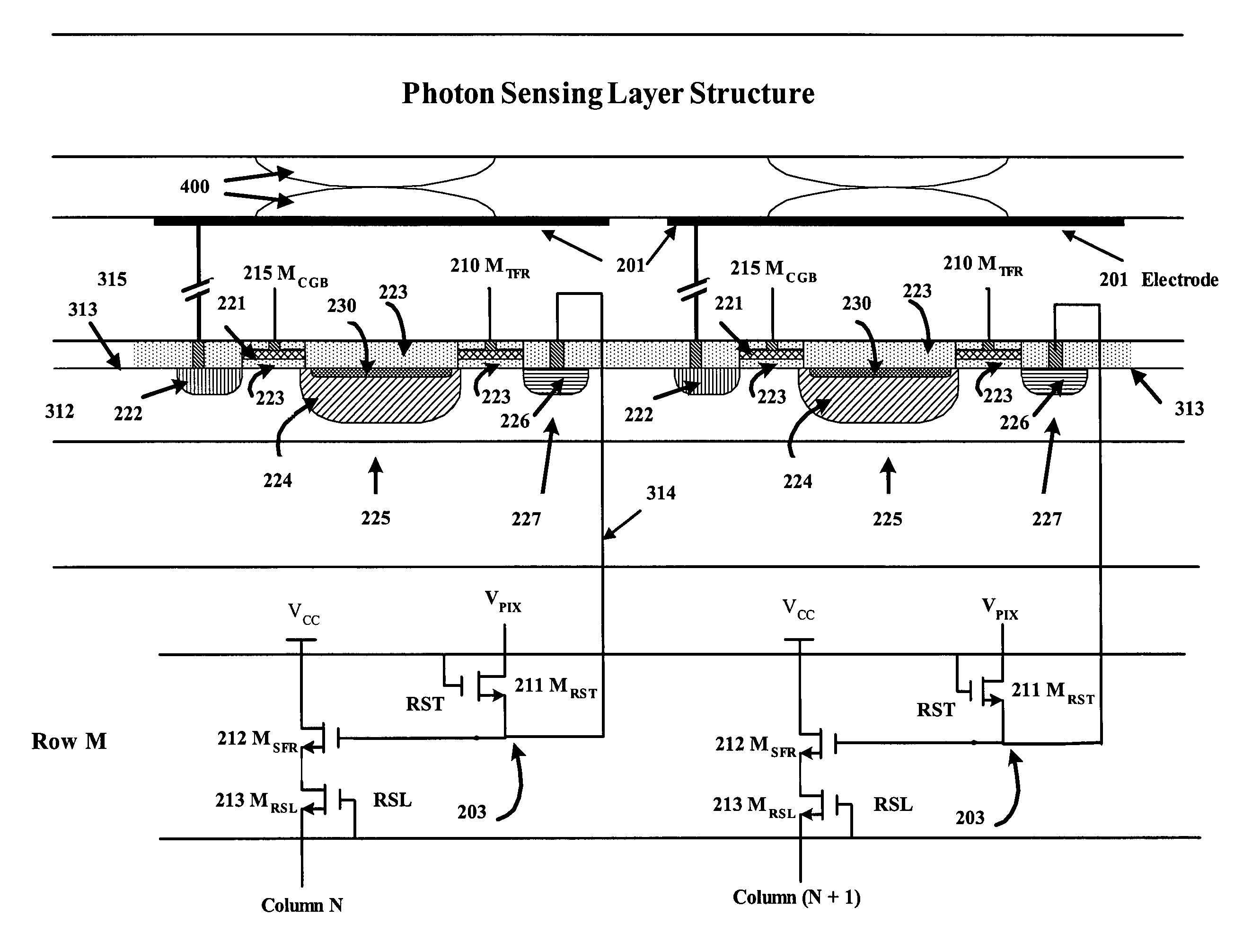
[0041]First and second preferred embodiments of the present invention are shown in FIGS. 9 and 10. This is a four transistor CMOS pixel circuit similar to pixel circuits described in the parent applications referred to in the second paragraph of this application. This pixel circuit may be one of many pixel circuits in an array of pixel circuits. The number could range from just a few pixels to several million pixels. For example Applicant and his fellow workers have designed and had fabricated sensors with 300 thousands, 2 millions, 36 million pixels and have even designed sensors with more than 150 million pixels.

[0042]This four transistor design includes a row select transistor 813 MRSL, a source follower transistor 812 MSFR, a reset transistor 811 MRST and a constant gate bias transistor 815 MCGB. The constant gate bias transistor assures that the pixel electrode at node 801 remains at a constant potential throughout the charge integration pr...


PUM


Abstract

A MOS or CMOS based active pixel sensor designed for operation with zero or close to zero potential across the pixel photodiodes to minimize or eliminate dark current. In preferred embodiments the pixel photodiodes are produced with a continuous pin or nip photodiode layer laid down over pixel electrodes of the sensor. In this preferred embodiment, the voltage potential across the pixel photodiode structures is maintained constant and close to zero, preferably less than 1.0 volts. This preferred embodiment enables the photodiode to be operated at a constant bias condition during the charge detection cycle. Setting this constant bias condition close to zero (near “short circuit” condition) assures that dark current is substantially zero.

Description

CROSS REFERENCE TO RELATED APPLICATIONS[0001]This application is a continuation-in-part of U.S. patent application Ser. No. 10 / 229,953 filed Aug. 27, 2002 now abandoned and U.S. patent application Ser. No. 10 / 229,955 filed Aug. 27, 2002 , now U.S. Pat. No. 7,411,233 and U.S. patent application Ser. No. 11 / 893,828 filed Aug. 17, 2007.[0002]The present invention relates to CMOS imaging sensors and in particular to such sensors with special sampling features for eliminating dark current noise.BACKGROUND OF THE INVENTIONCMOS Sensors[0003]CMOS sensors are well known. An active-pixel sensor (APS) is an image sensor consisting of an integrated circuit containing an array of pixel sensors, each containing a photodetector and connecting to an active transistor reset and readout circuit. Such an image sensor is produced by a CMOS process, and has emerged as an inexpensive alternative to charge-coupled device (CCD) imagers. The APS pixel solves the speed and scalability issues of the passive-p...

Claims


Application Information

Patent Timeline
Patent Type & Authority Patents(United States)
IPC IPC(8): H01L31/00
CPCH01L27/14609H01L27/14618H01L27/14667H04N3/155H04N3/1568H04N5/3575H04N5/361H04N5/363H04N5/374H04N5/37457H01L2924/0002H04N25/616H04N25/65H04N25/63H04N25/778H04N25/76H01L2924/00
Inventor HSIEH, TZU-CHIANG
Owner E PHOCUS
Why Eureka
Try Eureka