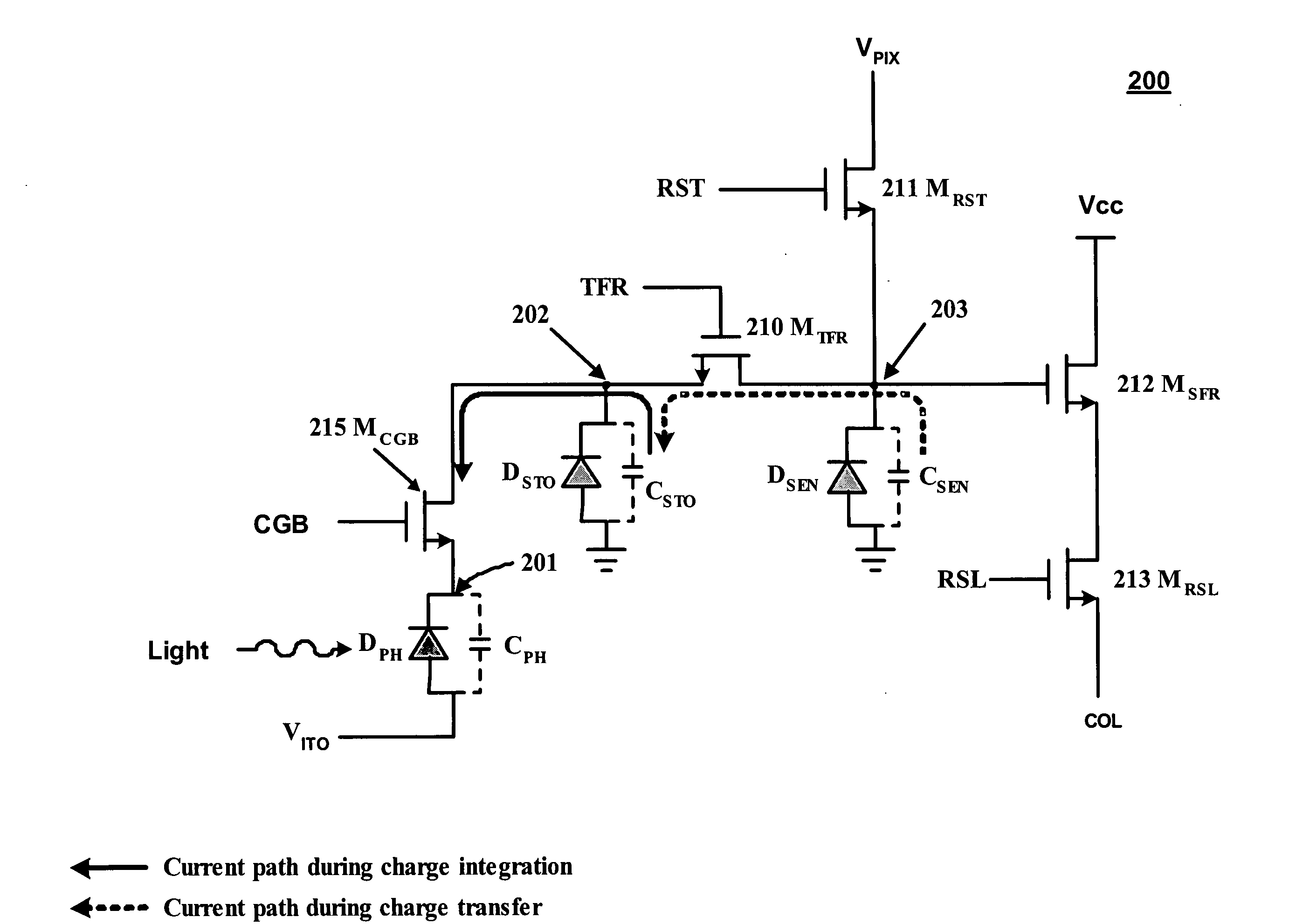
[0025]The present invention provides a MOS or CMOS based active pixel sensor designed for operation with zero or close to zero potential across the pixel photodiodes to minimize or eliminate dark current. In preferred embodiments the pixel photodiodes are produced with a continuous pin or nip photodiode layer laid down over pixel electrodes of the sensor. In this preferred embodiment, the
voltage potential across the pixel photodiode structures is maintained constant and close to zero, preferably less than 1.0 volts. This preferred embodiment enables the photodiode to be operated at a constant bias condition during the
charge detection cycle. Setting this constant bias condition close to zero (near “
short circuit” condition) assures that dark current is substantially zero.
[0026]In other preferred embodiments in addition to minimizing or eliminating dark current with zero or close to zero potential across the pixel photodiodes, the sensor is provided with special sampling features to substantially eliminate
clock noise. The sensor includes an array of pixels fabricated in or on a substrate, each pixel defining a charge collection node on which charges generated inside a photodiode region are collected, a charge integration node, at which charges generated in said pixel are integrated to produce pixel signals, a charge sensing node from which reset signals and the pixel signals are sensed. In preferred embodiments the sensor includes a continuous
electromagnetic radiation detection structure located above the pixel circuits providing a photodiode region for each pixel. The sensor includes
integrated circuit elements adapted to maintain
voltage potentials at the charge collection nodes substantially constant during charge integration cycles. The sensor also includes
integrated circuit elements having electrical
capacitance adapted to store charges providing an electrical potential at the charge integration node. In preferred embodiments this is a pinned
diode. The sensor also includes a
transfer switch to transfer charges from the charge integration node to the charge sensing node. The sensor also includes integrated circuit elements having electrical
capacitance adapted to store charges providing an electrical potential at the charge sensing node. The sensor also includes integrated circuit elements adapted to reset the charge sensing node and the charge integration node, integrated circuit elements adapted to convert the charges on the charge sensing node into electrical
signal, and integrated circuit elements adapted to readout electrical signals generated in the pixels.
[0027]One of the very important features of preferred embodiments of this invention is that the charge integration node and charge sensing node are separated from each other. This feature permits
correlated double sampling that basically eliminate clock noise as a problem.
[0029]This novel design resolves the concern of incomplete charge transfer on the charges stored on the photodiode (and its associated circuitry) since there is no charge transfer from the photodiode region during the
signal readout cycles. This is especially important if the photodiode is on pixel circuitry (like POAP) where the charges stored on the photodiode needs to travel through vias and interlayer
metal connectors in order to get to the charge sensing node. This travel path can not be fabricated with perfection in real practice; therefore, incomplete charge transfer is expected. Using a constant gate bias transistor to maintain the charge collection node at a constant value, eliminates the need of using the
effective capacitance of the photodiode and any fringe
capacitance along the conducting path from the photodiode to the charge collection node as a part of a charge integration capacitance. Therefore, since charges are not stored at, and readout from, the charge collection node; any imperfection of the path will not affect the
signal integrity of the signal.
[0030]However, it is as important to provide substantially complete charge transfer from the charge integration node to the charge sensing node. To do this, Applicant in preferred embodiments heavily dopes the integration node storage p-n
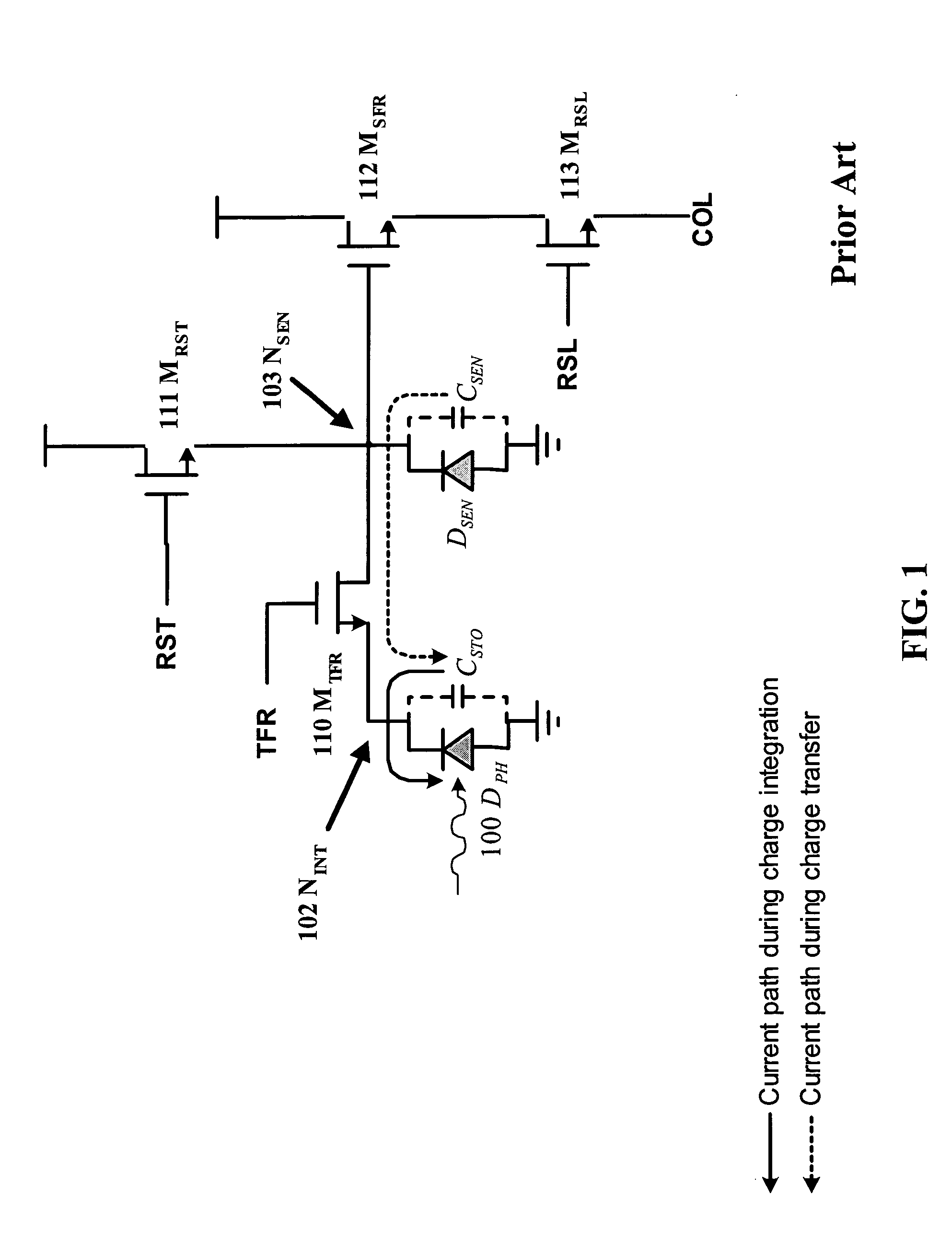
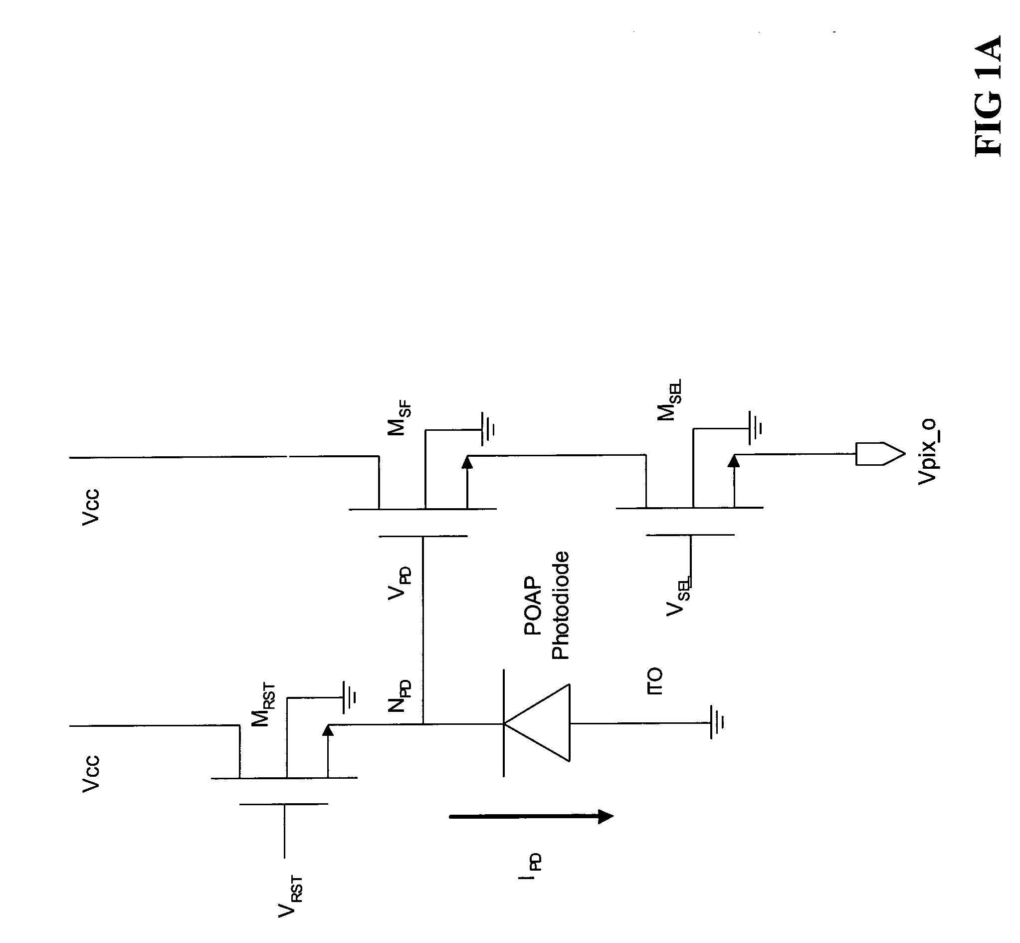
diode at the surface to fill the surface regions with holes to avoid or minimize electrons being trapped by the surface defects. This present invention uses only 5 transistors to provide CDS capability for Applicant's POAP pixel architecture. Applicant believes this invention provides an imaging sensor with the world highest sensitivity compared to all prior arts, including three-transistor CMOS, four-transistor CMOS with pinned photodiode and three-transistor POAP. The Applicants' present invention can also work as an “
electronic shutter” which could not be provided by other CDS-capable sensors found in the prior art.


