Electronic shutter using buried layers and active pixel sensor and array employing same

Inactive Publication Date: 2006-09-19
FOVEON
View PDF4 Cites 63 Cited by
  • Summary
  • Abstract
  • Description
  • Claims
  • Application Information

AI Technical Summary

Benefits of technology

[0014]Compatibility with advanced CMOS processes, the ability to perform long exposures, better noise and dynamic range performance, as well

Problems solved by technology

In either case, the resulting image can suffer from noticeable artifacts, particularly if objects in the scene are moving.
One of the fundamental limitations of electronic shutters implemented in electronic cameras using advanced CMOS is the need to place the shutter switch in a heavily doped surface well.
These high doping levels result in larger electric fields, particularly if signal voltages compatible with competitive imager dynamic ra

Method used


Image

  • Electronic shutter using buried layers and active pixel sensor and array employing same
  • Electronic shutter using buried layers and active pixel sensor and array employing same
  • Electronic shutter using buried layers and active pixel sensor and array employing same

Examples


Embodiment Construction

[0028]Persons of ordinary skill in the art will realize that the following description of the present invention is illustrative only and not in any way limiting. Other embodiments of the invention will readily suggest themselves to such skilled persons having the benefit of this disclosure.

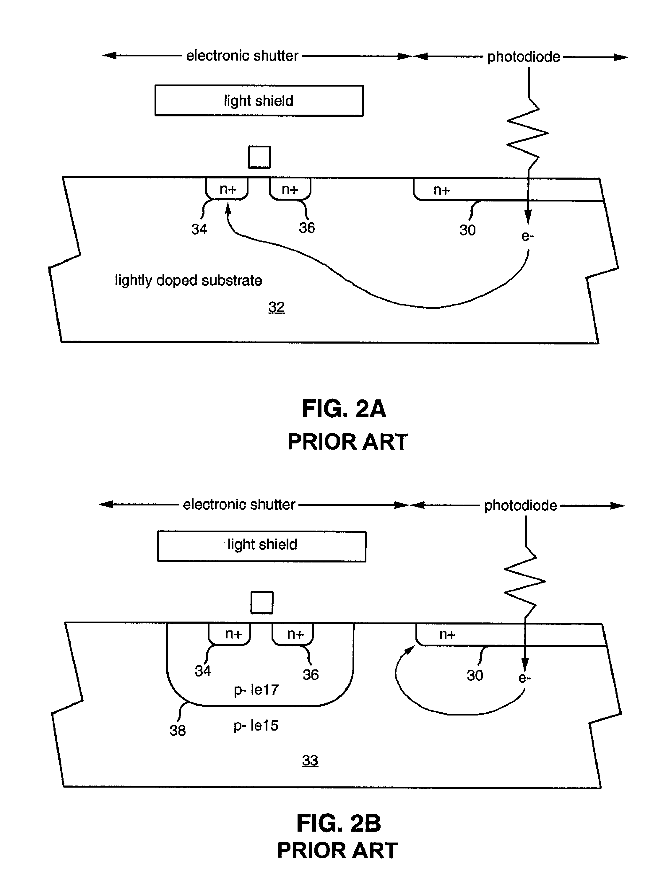
[0029]Referring now to FIG. 3, a semiconductor cross-sectional diagram shows an electronic shutter employing a buried layer to isolate the substrate from the transfer transistor that implements the electronic shutter switch. FIG. 3 uses the same reference numerals used in FIG. 2A to identify corresponding structures.

[0030]In FIG. 3, n+ region 30 and substrate 32 form the photodiode. In FIG. 3 the n+ source / drain regions 34 and 36 of the transfer transistor are located in the lightly doped p-substrate material and are isolated from the photodiode by using an n-type buried layer 42 and a surface n-well 44 in contact with buried layer 42 and surrounding the p-region in which n+ source / drain regions 3...


PUM


Abstract

An electronic shutter switching transistor for a CMOS electronic is formed in a semiconductor substrate of a first conductivity type. The transistor comprises a pair of spaced apart doped regions of a second conductivity type opposite the first conductivity type disposed in the semiconductor substrate forming source/drain regions. A gate is disposed above and insulated from the semiconductor substrate and is self aligned with the pair of spaced apart doped regions. A well of the second conductivity type laterally surrounds the pair of spaced apart doped regions and extends deeper into the substrate than the doped regions. A buried layer of the second conductivity type underlies and is in contact with the well.

Description

BACKGROUND OF THE INVENTION[0001]1. Field of the Invention[0002]The present invention relates to electronic cameras. More particularly, the present invention relates to CMOS electronic cameras with electronic shutters and to an improved electronic shutter using buried layers.[0003]2. The Prior Art[0004]Electronic cameras using imaging arrays are known in the art. Both CCD and CMOS imagers have been employed in such cameras.[0005]Some electronic cameras that employ CMOS active pixel sensors have employed such sensors equipped with an “electronic shutter” feature. The use of an electronic shutter is desirable because it eliminates the need for a mechanical shutter, reducing cost and complexity while improving the problem of latency between triggering an exposure and capturing an exposure. Electronic shutters in CMOS active pixel sensor arrays usually come in one of two forms: a rolling shutter or a true simultaneous shutter. A rolling shutter operates by successively exposing and rese...

Claims


Application Information

Patent Timeline
IPC IPC(8): H04N5/335
CPCH01L27/14603H01L27/14609H01L27/1463H04N5/335H01L27/14683H01L27/14647H01L27/14645H04N25/00
Inventor MERRILL, RICHARD B.
Owner FOVEON
Why Eureka
Try Eureka