Solid-state imaging element and camera system

Active Publication Date: 2010-01-21
SONY CORP
View PDF23 Cites 118 Cited by
  • Summary
  • Abstract
  • Description
  • Claims
  • Application Information

AI Technical Summary

Benefits of technology

[0031]The embodiments of the present invention can realize divided-pixel addition free from variation in the number of output electrons of the pixel with respect to the incident light amount. As a result, it is possible for the solid-

Problems solved by technology

However, in the case of the above-described divided-pixel addition, an invalid region (dead space) that does not directly contribute to photo-sensing exists in terms of signal processing diff

Method used


Image

  • Solid-state imaging element and camera system
  • Solid-state imaging element and camera system
  • Solid-state imaging element and camera system

Examples


Embodiment Construction

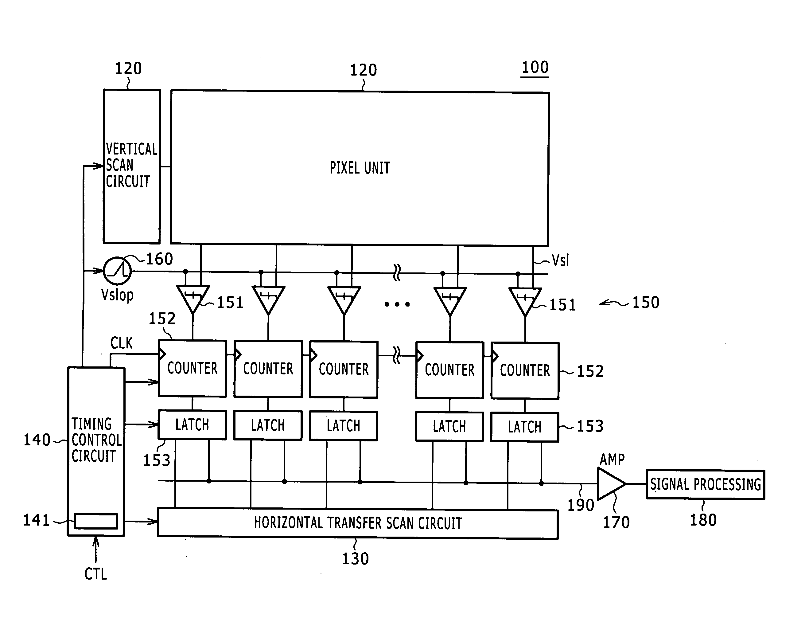
[0053]An embodiment of the present invention will be described below in association with the drawings.

[0054]FIG. 1 is a block diagram showing a configuration example of a solid-state imaging element (CMOS image sensor) including column parallel ADCs according to the embodiment of the present invention.

[0055]The embodiment of the present invention can be applied not only to the CMOS image sensor but also to a CCD. The following description will be made by taking the CMOS image sensor as one example.

[0056]As shown in FIG. 1, this solid-state imaging element 100 has a pixel unit 110, a vertical scan circuit 120, a horizontal transfer scan circuit 130, a timing control circuit 140, and an analog-digital converter (ADC) group 150.

[0057]The solid-state imaging element 100 further has a digital-analog converter (DAC) 160, amplifier circuits (S / A) 170, a signal processing circuit 180, and a horizontal transfer line 190.

[0058]The pixel signal readout unit is formed by the vertical scan circu...


PUM


Abstract

Disclosed herein is a solid-state imaging element including a pixel unit configured to include a plurality of pixels arranged in a matrix and a pixel signal readout unit configured to include an analog-digital conversion unit that carries out analog-digital conversion of a pixel signal read out from the pixel unit. Each one of the pixels in the pixel unit includes a plurality of divided pixels arising from division into regions different from each other in optical sensitivity or a charge accumulation amount. The pixel signal readout unit reads out divided-pixel signals of the divided pixels in the pixel. The analog-digital conversion unit carries out analog-digital conversion of the divided-pixel signals that are read out and adds the divided-pixel signals to each other to obtain a pixel signal of one pixel.

Description

BACKGROUND OF THE INVENTION[0001]1. Field of the Invention[0002]The present invention relates to a solid-state imaging element typified by a CCD and a CMOS image sensor, and a camera system.[0003]2. Description of the Related Art[0004]It is desired to realize a wide dynamic range solid-state imaging element by which even details can be so imaged that high-luminance information does not collapse and low-luminance part of the subject image does not become too black even in photographing against light such as light of car headlights, illumination light of a ball game ground, or sunlight.[0005]Under such circumstances, regarding a solid-state imaging element such as a CCD, techniques for enlarging the dynamic range are disclosed in e.g. Japanese Patent No. 2125710, Japanese Patent Laid-Open No. Hei 3-117281, Japanese Patent Laid-Open No. Hei 9-205589, and Japanese Patent Laid-Open No. 2004-320119 (Hereinafter, Patent Document 1, Patent Document 2, Patent Document 3, and Patent Document ...

Claims


Application Information

Patent Timeline
IPC IPC(8): H04N5/335H04N5/347H04N5/369H04N5/372H04N5/374H04N5/376H04N5/378H04N9/07
CPCH04N5/35545H04N5/378H04N5/37457H01L27/14627H01L27/14643H04N25/581H04N25/778H04N25/75
Inventor UI, HIROKI
Owner SONY CORP
Why Eureka
Try Eureka