Imaging device and electronic device

a technology of electronic devices and imaging devices, applied in the direction of radio frequency controlled devices, television systems, transistors, etc., can solve the problems of difficult to reduce the variation in electrical characteristics, the difficulty of a transistor manufacturing process increasing, and the total imaging time becoming long. , to achieve the effect of high sensitivity, wide dynamic range, and high quality imaging data

Active Publication Date: 2016-05-12
SEMICON ENERGY LAB CO LTD
View PDF5 Cites 22 Cited by
  • Summary
  • Abstract
  • Description
  • Claims
  • Application Information

AI Technical Summary

Benefits of technology

[0020]According to one embodiment of the present invention, an imaging device capable of obtaining high-quality imaging data can be provided. An imaging device capable of compensating variation in electrical characteristics of an amplifier transistor included in a pixel circuit can be provided. A low-power imaging device can be provided. An imaging device that is suitable for high-speed operation can be provided. An imaging device with high sensitivity can be provided. An imaging device with a wide dynamic range can be provided. An imaging device with high resolution can be provided. An imaging device formed at low cost can be provided. An imaging device with high reliability can be provided. A novel imaging device or the like can be provided. A novel semiconductor device or the like can be provided.

Problems solved by technology

However, as miniaturization progresses, the degree of difficulty of a transistor manufacturing process increases, and it is difficult to reduce variation in electrical characteristics.
However, total imaging time becomes long if data is written to a capacitor by each imaging.
In addition, the increase in power consumption becomes a problem.

Method used


Image

  • Imaging device and electronic device
  • Imaging device and electronic device
  • Imaging device and electronic device

Examples


embodiment 1

[0083]In this embodiment, an imaging device that is one embodiment of the present invention is described with reference to drawings.

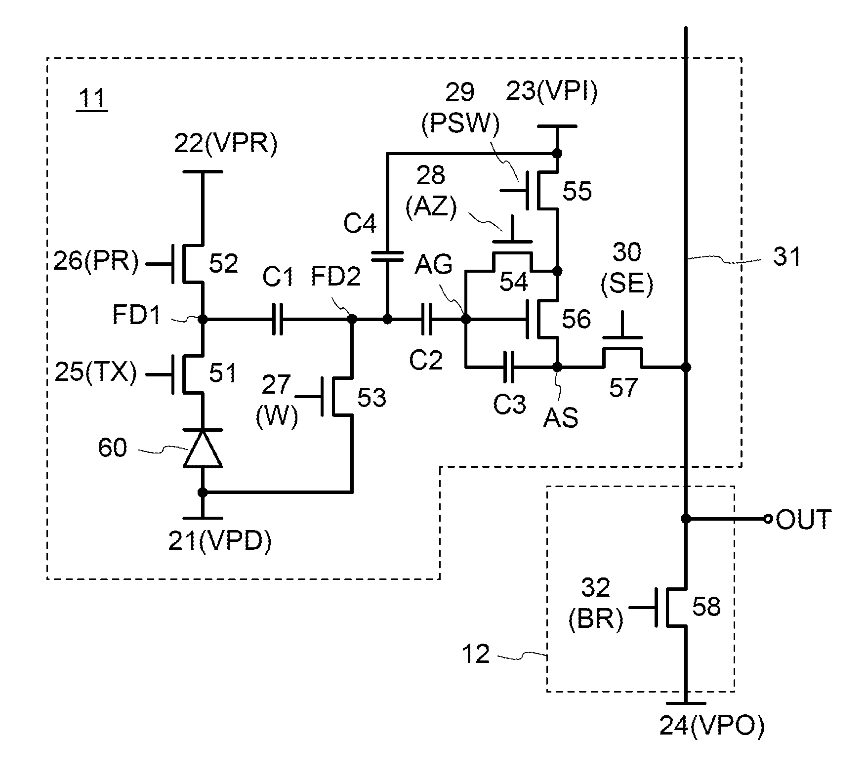
[0084]An imaging device in one embodiment of the present invention includes a pixel circuit that can compensate variation in threshold voltage of a source follower amplifier transistor in a pixel of an imaging device that outputs signal charge (data) by a source follower.

[0085]FIG. 1 is a circuit diagram of a circuit 11 that can function as a pixel circuit and a circuit 12 that can function as a reference current source circuit included in an imaging device in one embodiment of the present invention. In FIG. 1 and the like, transistors are n-ch transistors; however, one embodiment of the present invention is not limited thereto. The transistors may be p-ch transistors by reversing the magnitude relationship of a potential as illustrated in FIG. 47. Alternatively, some of the n-ch transistors may be replaced with p-ch transistors.

[0086]The circuit 11 is ...

embodiment 2

[0166]In this embodiment, an example of a method for driving a pixel circuit is described.

[0167]The pixel circuit described in Embodiment 1 can perform first operation in which normal imaging is performed and second operation in which differential data of imaging data of an initial frame and imaging data of a current frame can be retained and a signal based on the differential data can be output. In the second operation, differential data can be output without a comparison process or the like in an external circuit; thus, the pixel circuit can be applied to a low-power security camera or the like.

[0168]As illustrated in FIGS. 17A and 17B, an imaging device in one embodiment of the present invention includes a pixel portion 400 that includes the circuits 11 arranged in a matrix, a row driver 410 connected to the circuits 11, the circuits 12 connected to the circuits 11, an A / D converter 420 connected to the circuits 12, and a column driver 430 connected to the A / D converter 420. The ...

embodiment 3

[0185]In this embodiment, an example of a method for driving a pixel circuit is described.

[0186]As described in Embodiment 2, the operation of the pixel circuit is repetition of the reset operation, the accumulation operation, and the selection operation. As imaging modes in which the whole pixel matrix is controlled, a global shutter system and a rolling shutter system are known.

[0187]FIG. 20A is a timing chart of a global shutter system. The timing chart illustrates operation of an imaging device in which a plurality of pixel circuits in FIG. 1 are arranged in a matrix. Specifically, the timing chart illustrates operation of the pixel circuits from a first row to an n-th row (n is a natural number of 3 or more). The operation is described giving the first operation described in Embodiment 2 as an example.

[0188]In FIG. 20A, a signal 501, a signal 502, and a signal 503 are input to the wirings 26 (PR) connected to the pixel circuits in the first row, the second row, and the n-th row...


PUM


Abstract

To provide an imaging device capable of obtaining high-quality imaging data. The imaging device includes a first circuit and a second circuit. The first circuit includes a photoelectric conversion element, a first transistor, a second transistor, a third transistor, a fourth transistor, a fifth transistor, a sixth transistor, a seventh transistor, a first capacitor, a second capacitor, and a third capacitor. The second circuit includes an eighth transistor. The imaging device can compensate variation in threshold voltage of an amplifier transistor included in the first circuit.

Description

BACKGROUND OF THE INVENTION[0001]1. Field of the Invention[0002]One embodiment of the present invention relates to an imaging device.[0003]Note that one embodiment of the present invention is not limited to the above technical field. The technical field of one embodiment of the invention disclosed in this specification and the like relates to an object, a method, or a manufacturing method. One embodiment of the present invention relates to a process, a machine, manufacture, or a composition of matter. Specifically, examples of the technical field of one embodiment of the present invention disclosed in this specification include a semiconductor device, a display device, a liquid crystal display device, a light-emitting device, a lighting device, a power storage device, a storage device, an imaging device, a method for driving any of them, and a method for manufacturing any of them.[0004]In this specification and the like, a semiconductor device generally means a device that can funct...

Claims


Application Information

Patent Timeline
Patent Type & Authority Applications(United States)
IPC IPC(8): H04N5/225H01L27/146
CPCH01L27/14612H04N5/2253H01L27/14692H01L27/14665H01L27/14643H04N25/771H04N25/70H04N25/75H04N23/54
Inventor INOUE, HIROKIKUROKAWA, YOSHIYUKIIKEDA, TAKAYUKIOKAMOTO, YUKI
Owner SEMICON ENERGY LAB CO LTD
Why Eureka
Try Eureka