Charge transfer apparatus

a technology of charge transfer and discharge device, which is applied in the direction of radio frequency control devices, instruments, television systems, etc., can solve the problems of difficult application of large potential gradients, ccd or csd used in solid-state image pickup elements, etc., and achieve wide dynamic range and high sensitivity

Inactive Publication Date: 2005-04-05
CANON KK
View PDF16 Cites 23 Cited by
  • Summary
  • Abstract
  • Description
  • Claims
  • Application Information

AI Technical Summary

Benefits of technology

It is another object of the present invention to provide an image pickup apparatus capable of high-speed signal read-out with high sensitivity and wide dynamic range.

Problems solved by technology

However, the CCD or CSD used in a solid-state image pickup element suffers the following problem.
However, the CSD can transfer only a set of signal charges at once, its operation is inevitably line-sequential driving, and the signal charges of photodiodes on a row selected for signal transfer must be transferred at high speed.
(1) Since the capacitance between the MOS electrode and the semiconductor interface and that between the semiconductor interface and the semiconductor bulk are connected in series, only a value obtained by multiplying the potential gradient supplied to the MOS electrode by the capacitance division ratio is applied to the semiconductor interface. This capacitance division ratio is generally as low as about 0.1 to 0.3.
(2) Since the potential gradient supplied to the MOS electrode introduces an ohmic current through this portion, a large potential gradient is difficult to apply.
(3) The charge mobility at the semiconductor interface serving as a transfer path is lower than that in the semiconductor bulk.
The CSD is widely used in an infrared image pickup apparatus which must process a large amount of signal charges, but is difficult due to those problems to use in an image pickup apparatus for a visible region with a high signal read-out speed.

Method used


Image

  • Charge transfer apparatus
  • Charge transfer apparatus
  • Charge transfer apparatus

Examples


second embodiment

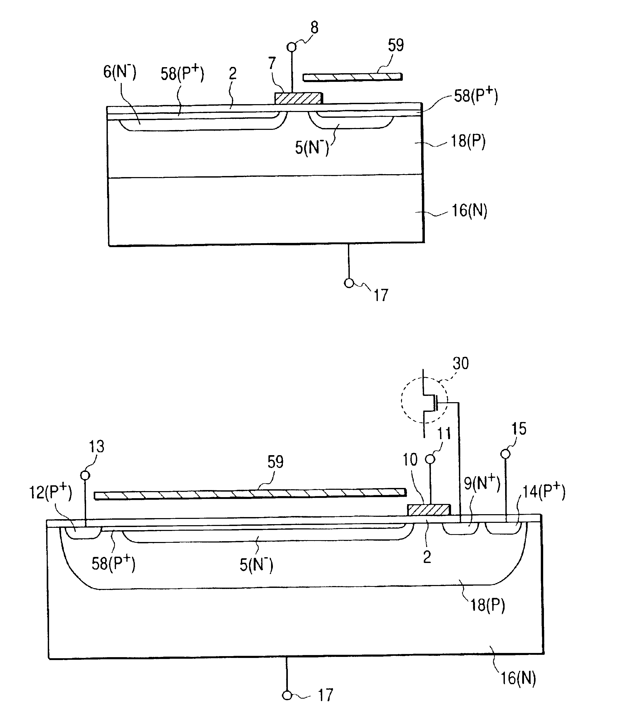
In the second embodiment, the n-type substrate and p-type well are electrically isolated, so that another electrical element can be independently formed at a location other than the p-type well where the charge transfer apparatus is formed.

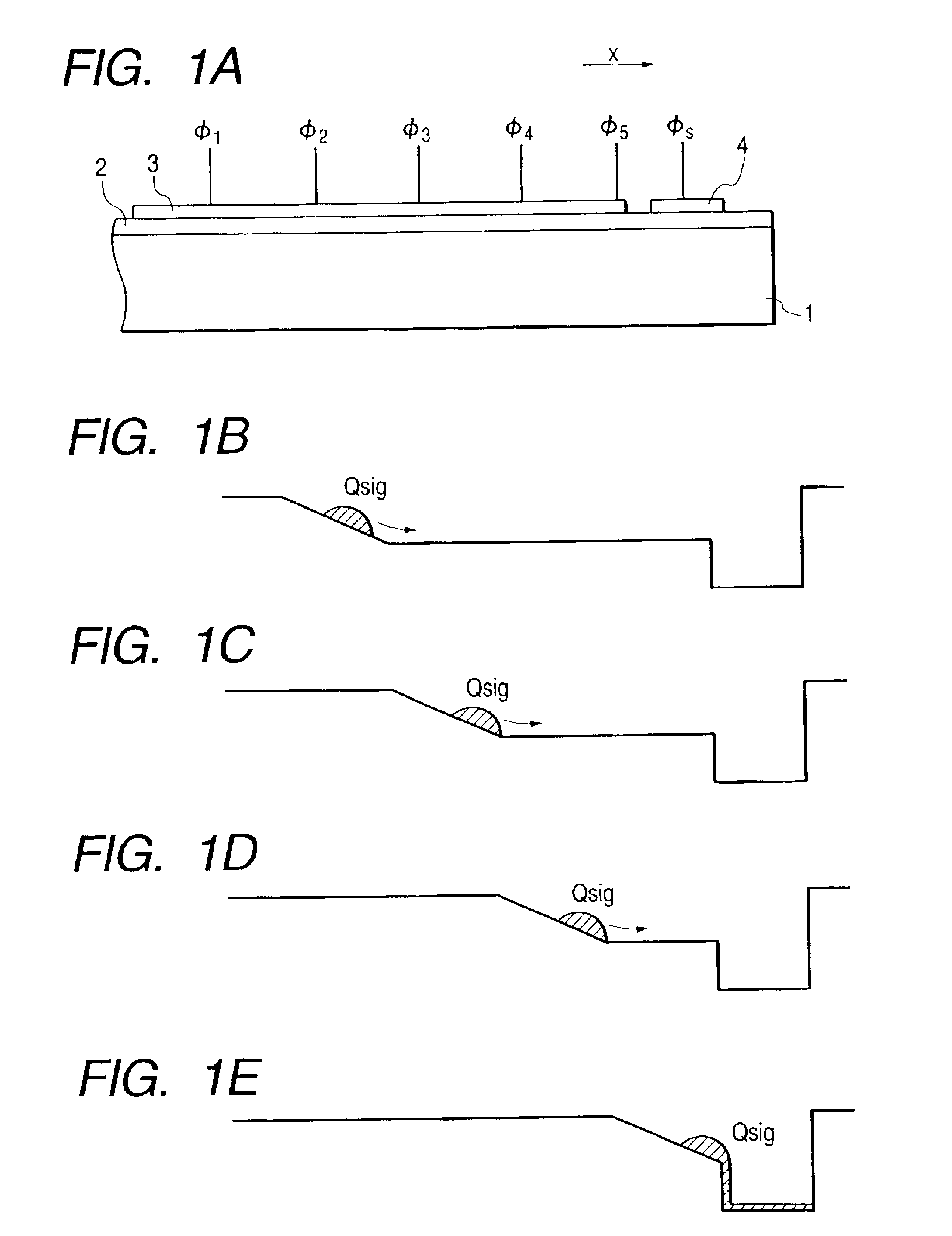
FIG. 4A is a sectional view of a charge transfer element according to the third embodiment of the present invention, and FIGS. 4B to 4E are views of the potentials showing the transfer method.

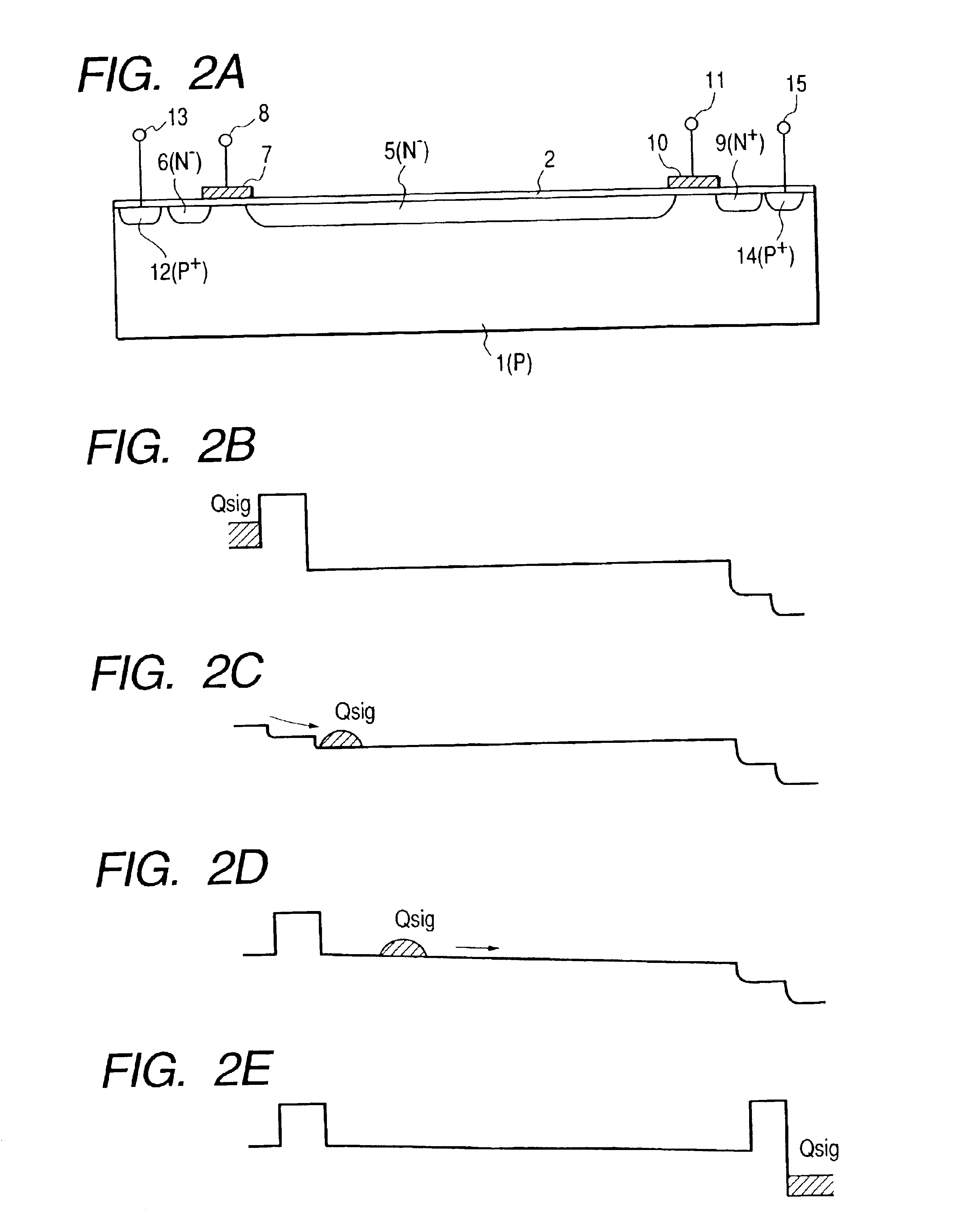
In FIG. 4A, p-type semiconductor regions 19 and 20 are formed near a charge transfer region 5 to ohmic-contact a p-type substrate 1, and are aligned in the charge transfer direction (X direction in FIG. 4A). The semiconductor regions 19 and 20 overlap the charge transfer region 5 in FIG. 4A, but are indicated by dotted lines to represent that they are located slightly apart from the charge transfer region 5 in a direction perpendicular to the sheet surface of FIGS. 4A to 4D. Terminals 21 and 22 apply potentials to the semiconductor regions 19 and 20. In FIG. ...

sixth embodiment

the present invention relates to an application of the charge transfer element of the second embodiment to an amplifier type solid-state image pickup element. In the amplifier type solid-state image pickup element, signal charges accumulated in a light-receiving pixel are guided to the control electrode of a transistor formed in a pixel, and an amplified signal is output from a main electrode. Amplifier type transistors are for example, an SIT image sensor using an SIT (A. Yusa, J. Nishizawa et al., “SIT image sensor: Design consideration and characteristics”, IEEE trans. Vol. ED-33, pp. 735-742, June 1986), a BASIS using a bipolar transistor (N. Tanaka et al., “A 310K pixel bipolar imager (BASIS)”, IEEE Trans. Electron Devices, Vol. 35, pp. 646-652, May 1990), a CMD using a JFET whose control electrode is depleted (Nakamura et al., “Gate accumulation type MOS phototransistor image sensor”, Journal of Television Society, 41, 11, pp. 1,075-1,082, November, 1987), and a CMOS sensor us...


PUM


Abstract

To transfer signal charges at high speed with small noise, there is provided a charge transfer apparatus including a semiconductor substrate of one conductivity type, a charge transfer region of a conductivity type opposite to that of the semiconductor substrate that is formed in the semiconductor substrate and joined to the semiconductor substrate to form a diode, a signal charge input portion which inputs a signal charge to the charge transfer region, a signal charge output portion which accumulates the signal charge transferred from the charge transfer region, and a plurality of independent potential supply terminals which supply a potential gradient to the semiconductor substrate, wherein the signal charge in the charge transfer region is transferred by the potential gradient formed by the plurality of potential supply terminals.

Description

BACKGROUND OF THE INVENTION1. Field of the InventionThe present invention relates to a charge transfer apparatus for transferring charges, and an image pickup apparatus using the same.2. Related Background ArtConventional charge transfer elements are a CCD (Charge Coupled Device) and CSD (Charge Sweep Device; Japanese Patent Publication No. 63-38866 and Japanese Laid-Open Patent Application No. 2-63314), and are mainly applied to solid-state image pickup elements. These charge transfer elements consist of MOS diodes formed on a semiconductor, and receive signal charges in depletion layers formed near the semiconductor interface by controlling the gate electrode potentials of the MOSs. The CCD and CSD adopt different transfer methods. The CCD is constituted by forming multistage MOS diodes, a potential well is formed on each stage, and a plurality of independent signal charges are assigned to a plurality of potential wells. The gate electrode potential of MOS on the respective stage ...

Claims


Application Information

Patent Timeline
Patent Type & Authority Patents(United States)
IPC IPC(8): H01L27/148H04N5/335H04N5/355H04N5/369H04N5/372
CPCH01L27/1485H01L27/14818
Inventor SHINOHARA, MAHITO
Owner CANON KK
Why Eureka
Try Eureka