CMOS sensor array with a shared structure

a technology of complementary metaloxide semiconductors and which is applied in the field of layout of complementary metaloxide semiconductor can solve the problems of higher production costs and power consumption of ccd types compared to cmos types, and the limitation of forming the layout of active pixel sensor arrays having a shared structur

Active Publication Date: 2006-08-10
SAMSUNG ELECTRONICS CO LTD
View PDF3 Cites 63 Cited by
  • Summary
  • Abstract
  • Description
  • Claims
  • Application Information

AI Technical Summary

Problems solved by technology

The CCD active pixel sensor type generally exhibits less noise and better image quality than the CMOS active pixel sensor type, but the production costs and power consumption are higher for the CCD type as compared to the CMOS type.
In general, there are limitations to forming the layout of the active pixel sensor array having a shared structure.

Method used


Image

  • CMOS sensor array with a shared structure
  • CMOS sensor array with a shared structure
  • CMOS sensor array with a shared structure

Examples


Embodiment Construction

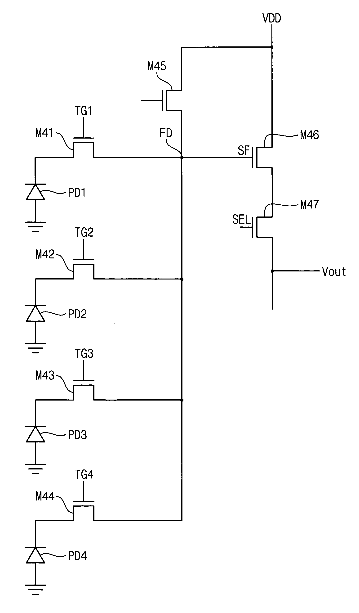
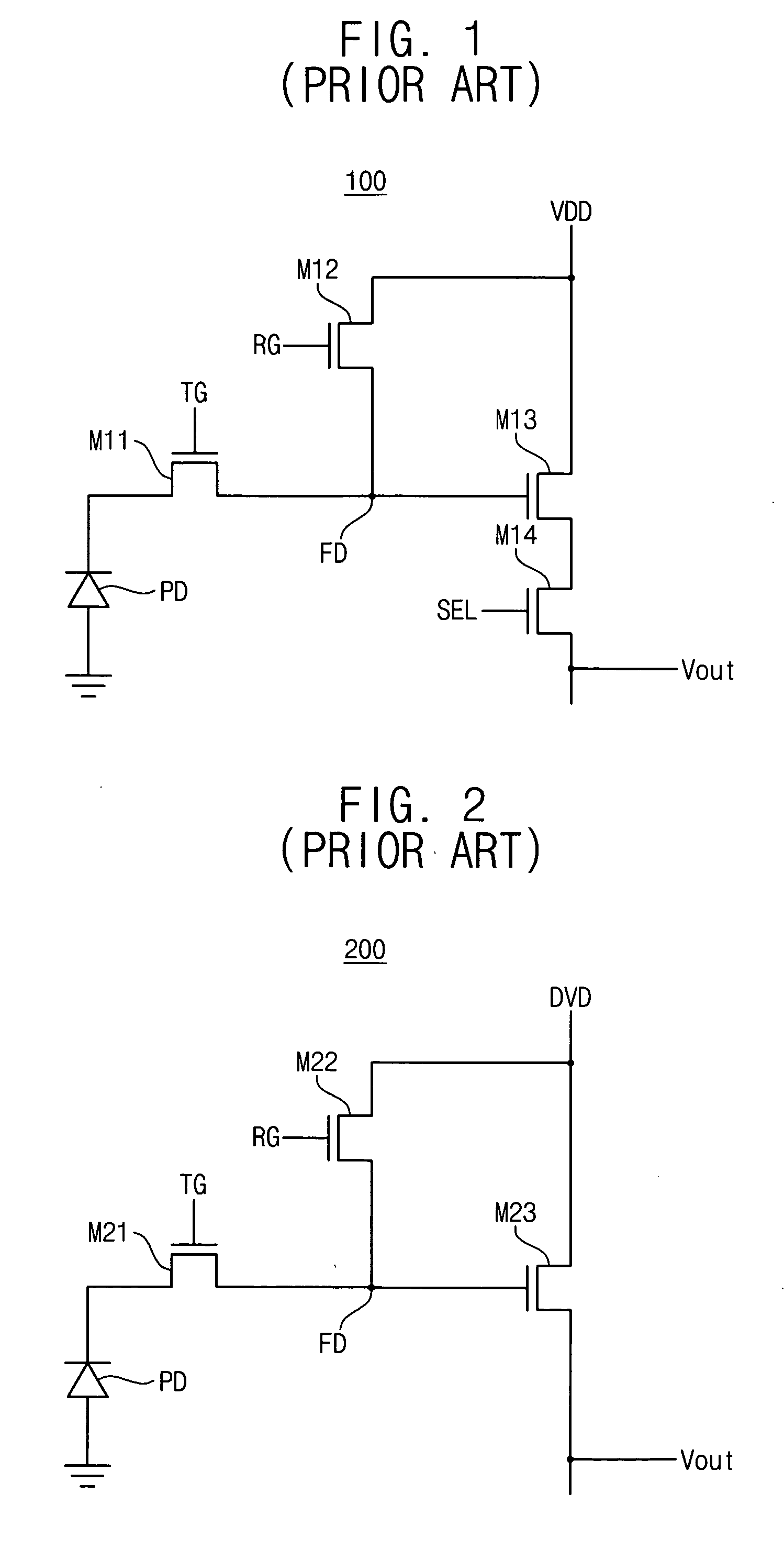
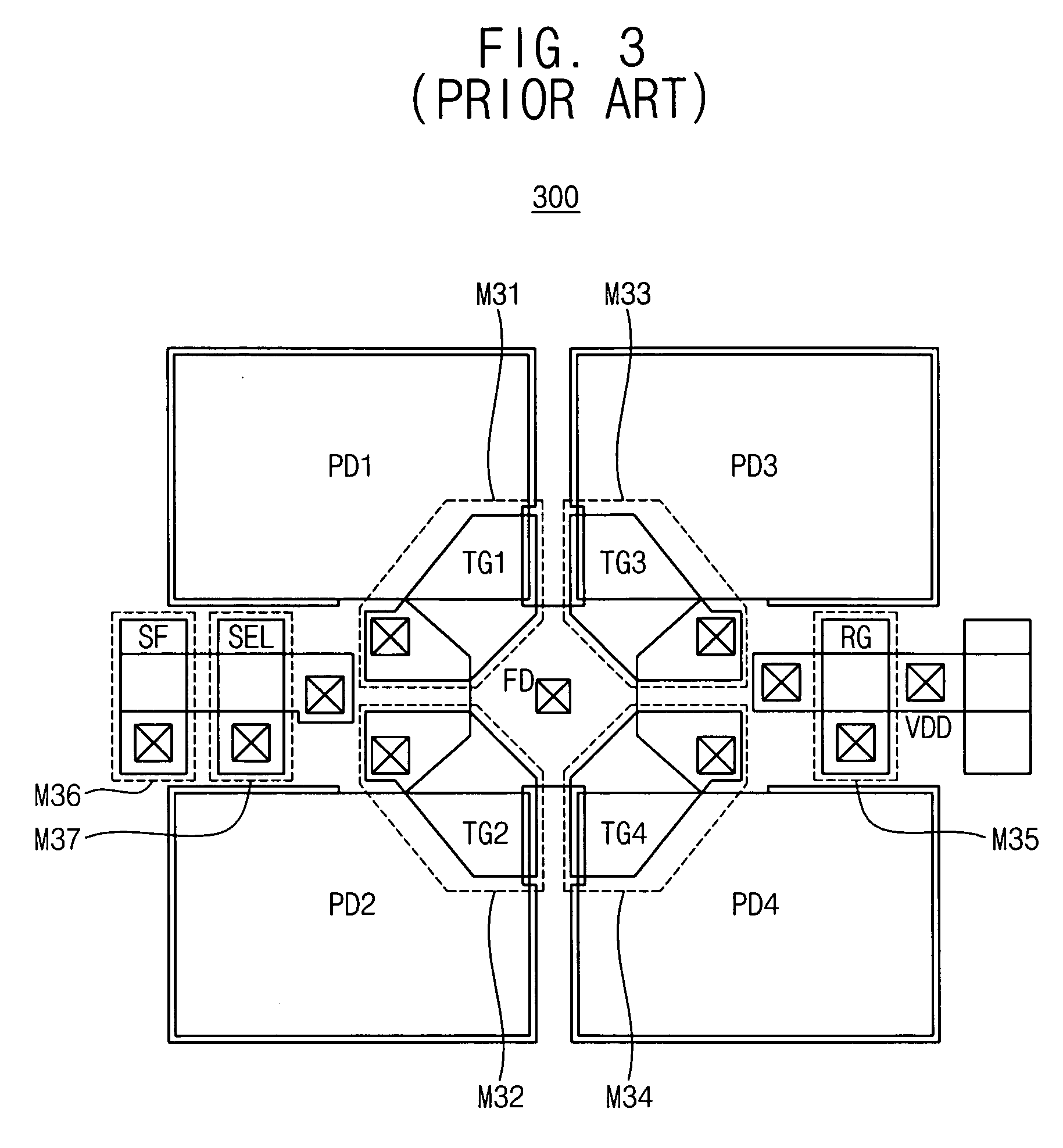
[0041] Hereinafter, the exemplary embodiments of the present invention will be described in detail with reference to the accompanying drawings. In the drawings, the size and relative sizes of layers and regions may be exaggerated for clarity. Like reference numerals refer to similar or identical elements throughout the description of the figures. As used herein, “natural numbers” are the numbers 1, 2, 3, . . . .

[0042] It will be understood that when an element or layer is referred to as being “on”, “connected to” or “coupled to” another element or layer, it can be directly on, connected or coupled to the other element or layer or intervening elements or layers may be present. As used herein, the term “and / or” includes any and all combinations of one or more of the associated listed items.

[0043] It will be understood that, although the terms first, second, etc. may be used herein to describe various elements, components, regions, layers and / or sections, these elements, components, ...


PUM


Abstract

A CMOS sensor array includes a plurality of unit blocks. A unit block includes: N pairs of photo diode regions arranged in a first direction; 2N transfer transistors respectively corresponding to the photo diode regions, wherein each of the transfer transistors is formed at a corner of the corresponding photo diode region, and wherein for each pair of photo diode regions the two corresponding transfer transistors symmetrically oppose each other; N floating diffusion nodes, wherein each of the floating diffusion nodes is respectively arranged between a pair of photo diode regions, and wherein each of the floating diffusion nodes is shared by the two corresponding transfer transistors and the pair of photo diode regions; at least one metal line for coupling the floating diffusion nodes; a reset transistor for resetting a voltage of the floating diffusion nodes; a readout circuit including at least one transistor for sampling the floating diffusion node, wherein the reset transistor and the readout circuit are disposed between the pair of photo diode regions.

Description

CROSS-REFERENCE TO RELATED APPLICATIONS [0001] This application claims priority to Korean Patent Application No. 10-2005-0011131, filed on Feb. 7, 2005, the contents of which are herein incorporated by reference in its entirety. BACKGROUND OF THE INVENTION [0002] 1. Technical Field [0003] The present invention relates to a layout of active pixel sensor arrays and, more particularly, to a layout of a complementary metal-oxide semiconductor (CMOS) active pixel sensor array having a shared structure in which a plurality of active pixel sensors share a reset transistor and readout transistors. [0004] 2. Description of the Related Art [0005] An active pixel sensor is a device for transforming a photo image into an electrical signal. Active pixel sensors are widely used in digital cameras, camera-mounted mobile phones, visual systems, etc. [0006] The active pixel sensor may be broadly classified into a charge-coupled device (CCD) active pixel sensor type and a complementary metal-oxide se...

Claims


Application Information

Patent Timeline
Patent Type & Authority Applications(United States)
IPC IPC(8): H01L27/00H01L27/146H04N5/335H04N5/369H04N5/374
CPCH01L27/14603H01L27/14609H01L27/14641H04N5/37457H01L27/14643H04N25/778H01L27/14
Inventor KIM, YOUNG-CHANKIM, YI-TAE
Owner SAMSUNG ELECTRONICS CO LTD
Why Eureka
Try Eureka