[0022]The present invention provides a
hybrid MOS or CMOS based
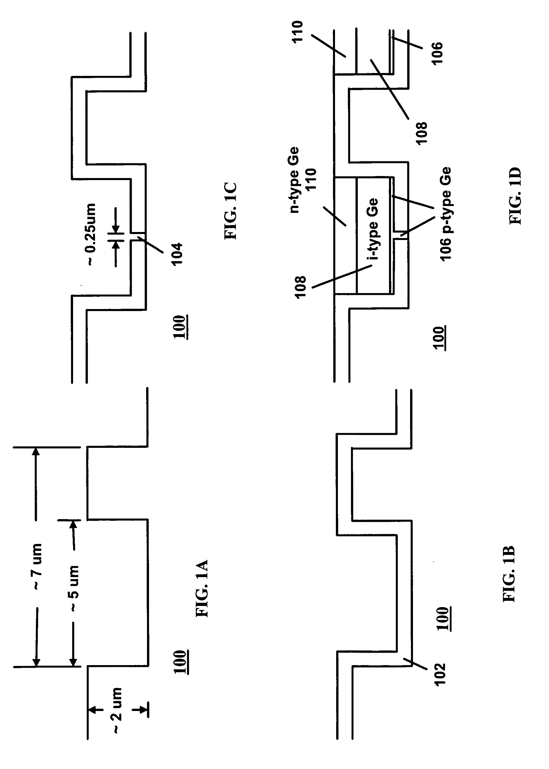
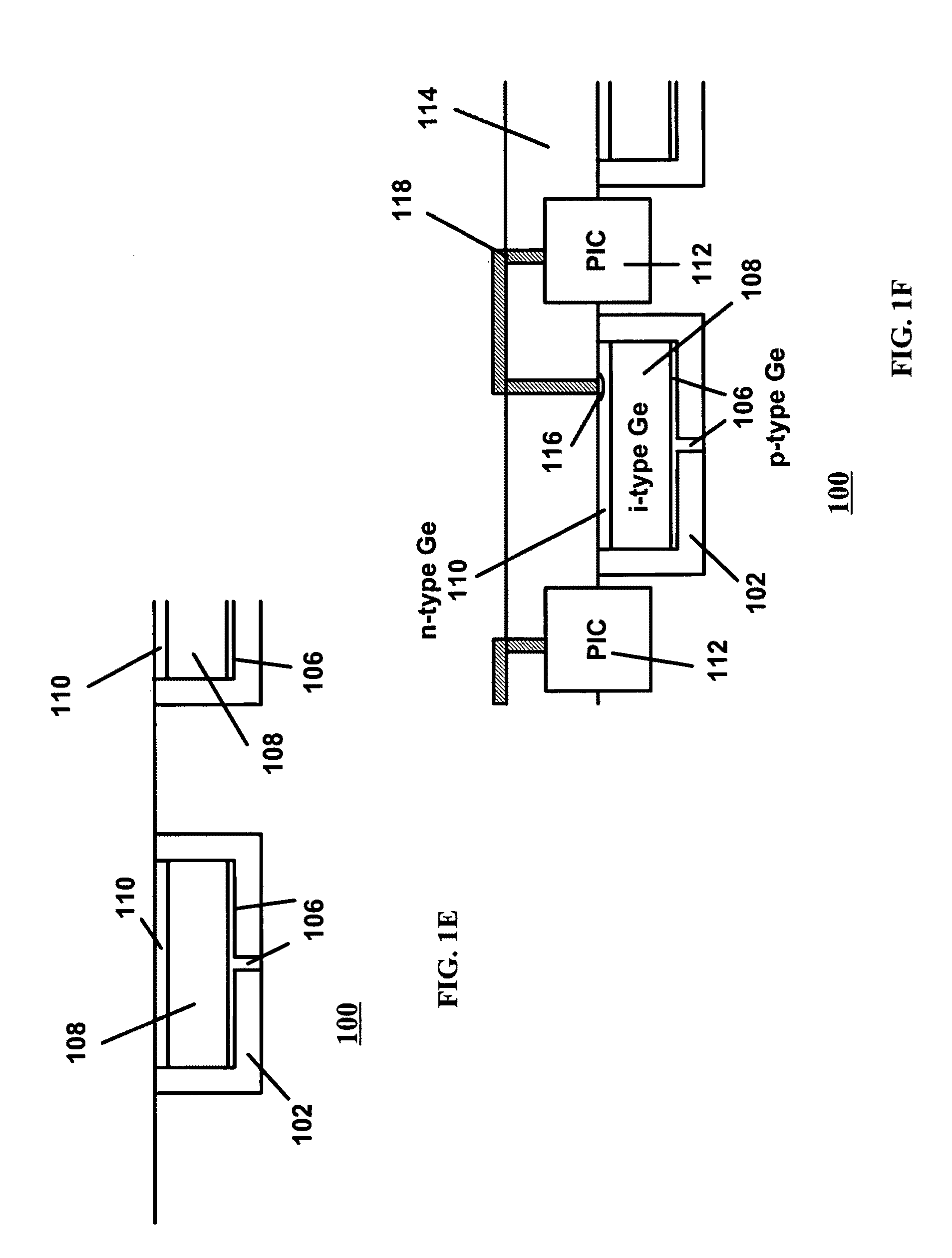
image sensor. The sensor includes photon-sensing elements comprised of an array of photo-sensing elements deposited in the form of separate islands on or in a substrate. Pixel circuitry is created on and / or in the
silicon substrate at or near the edge of or beneath the photon-sensing elements. The photo-sensing elements may be formed with a stack of photo-sensing semiconductor
layers or created in a single photon-sensing semiconductor layer. Special circuitry is provided to keep the potential across the pixel photon-sensing element at or near zero volts to minimize or eliminate
dark current. The
potential difference is preferably less than 1.0
volt. The circuitry also keeps the small potential difference across the photodiodes constant or approximately constant throughout the charge integration cycle. In preferred embodiments the substrate is a crystalline substrate and the photon-sensing elements are separated by a
dielectric layer from the substrate except for a
small hole through which the material of the photon-sensing element can be grown epitaxially. Photodiodes are used in the preferred embodiments as the photo-sensing elements.
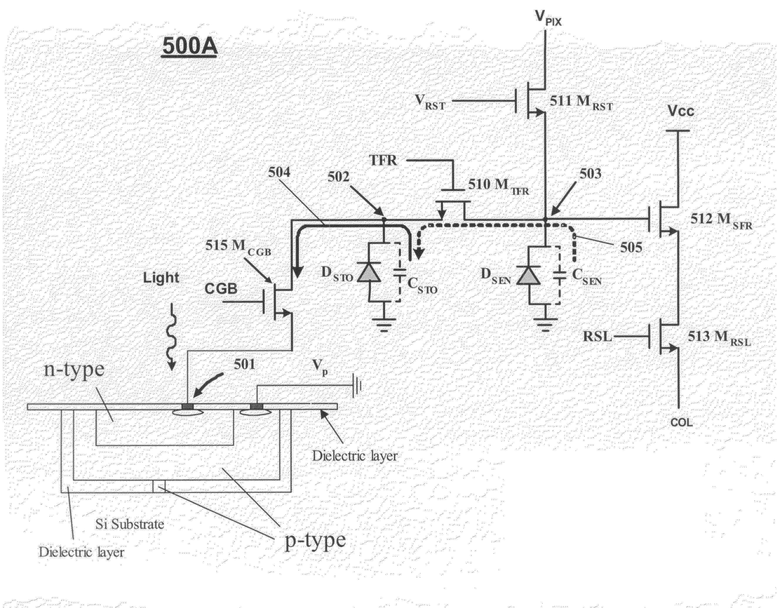
[0023]Preferred embodiments are adapted for
correlated double sampling to substantially reduce or eliminate
clock noise. Preferred embodiments include pixel circuitry defining a charge collection node on which charges generated inside a
photodiode region are collected, a charge integration node, at which charges generated in said pixel are integrated to produce pixel signals, a charge sensing node from which reset signals and the pixel signals are sensed. The charge collection node and charge integration node are physically separated from each other. However, the charge integration node and charge sensing node can be electrically shorted to be considered as a common node or separated by other circuit elements as two separated nodes. In this separation Applicant preferably uses a constant gate bias
transistor whose gate is held at a substantially constant bias
voltage, about 1.2 V, during the charge integration cycle. Applicant makes this bias
voltage programmable in the range of 0.7V to 2.1V to fine tune the overall sensor performance. This
transistor maintains the
voltage at the charge collection node at a constant value, at least during the charge integration cycle. The charge collection node is considered
electrically short to the one of the
electrode connecting to the photodiode. This
constant voltage eliminates the need to use the built-in
capacitance of the photodiode to store
signal charges. The
capacitance associated with the integration node is reset to produce a potential at the integration node of about 2.6 volts at the beginning of the charge integration cycle in the preferred embodiment. The constant gate bias
transistor allows current flowing from the charge integration node to the charge collection node until the charge collection node is charged up to slightly (a few tenths of a
volt) below the constant gate bias. After reset, the charge integration node is left “floating”.
[0025]This novel design resolves the concern of incomplete charge transfer on the charges stored on the photodiode (and its associated circuitry) since there is no charge transfer from the photodiode region during the
signal readout cycles. Charge transfer from photodiode regions during readout can be a serious problem where the charges stored on the photodiode needs to travel through vias and interlayer
metal connectors in order to get to the charge sensing node. This travel path can not be fabricated with perfection in real practice; therefore, incomplete charge transfer is expected. Using a constant gate bias transistor to maintain the charge collection node at a constant value, eliminates the need of relying on the
effective capacitance of the photodiode and fringe
capacitance along the conducting path from the photodiode to the charge collection node as a part of a charge integration capacitance. Therefore, since
signal charges are not stored at, and readout from, the charge collection node; any imperfection of the path will not affect the integrity of the signal. Use of the constant gate bias is also important where the photodiode material is naturally subject to dark current leakage.
[0026]It is as important to provide substantially complete charge transfer from the charge integration node to the charge sensing node. To do this, Applicant in preferred embodiments heavily dopes the surface of the storage n-p junction
diode to fill the surface regions with acceptors to avoid or minimize the
trapping and re-emission of electrons by the surface defects. In some preferred embodiments of the present invention five transistors per pixel are used to provide CDS capability.

