Multi-step surface passivation structures and methods for fabricating same

a surface passivation and multi-step technology, applied in semiconductor devices, semiconductor/solid-state device details, electrical devices, etc., can solve the problems of low gate leakage during device operation, single insulating passivation layer cannot do both at the same time, etc., to achieve the effect of reducing or eliminating leakage current and high electron density in the channel

Active Publication Date: 2017-12-07
EFFICIENT POWER CONVERSION CORP
View PDF2 Cites 10 Cited by
  • Summary
  • Abstract
  • Description
  • Claims
  • Application Information

AI Technical Summary

Benefits of technology

[0010]The present invention in the various embodiments described below addresses the problems discussed above and other problems, by providing a column III nitride transistor, preferably a GaN transistor, that includes two or more insulator semiconductor interface regions to minimize or eliminate leakage current and gate to drain capacitance, while the device exhibits high electron density in the channel and low drain field, during device conduction.

Problems solved by technology

In addition, using a compensated semiconductor layer 38 leads to low gate leakage during device operation.
But the single insulating passivation layer cannot be made to do both at the same time.

Method used


Image

  • Multi-step surface passivation structures and methods for fabricating same
  • Multi-step surface passivation structures and methods for fabricating same
  • Multi-step surface passivation structures and methods for fabricating same

Examples


first embodiment

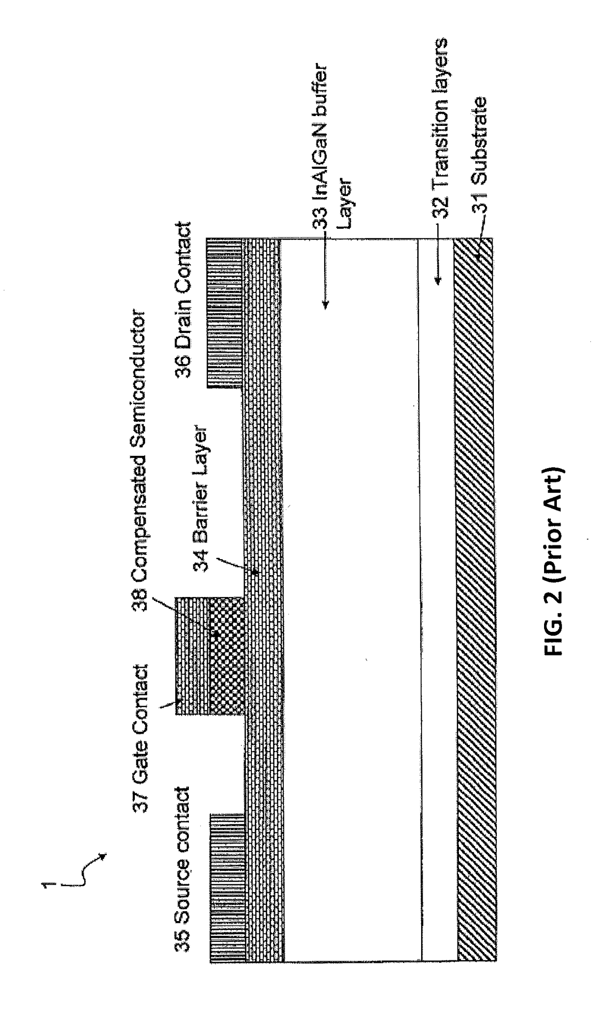
[0055]FIG. 3 illustrates a cross-sectional view of a GaN transistor 300 formed according to the present invention. A first insulator (insulator 139) is disposed between the gate and drain and above the barrier layer 134. First insulator 139 minimizes the gate leakage and fields near the gate that cause high gate-drain charge (Qgd). An adjacent second insulator (insulator 140) minimizes electric fields at the drain contact and provides a high density of charge in the channel for low resistance. The remaining elements / layers of this transistor may be, for example, those shown in the conventional transistor of FIG. 2, as described above, and thus are hereby incorporated within this and other sections of the detailed description. These elements / layers include substrate 131, transition layers 132, buffer layer 133, source contact 135, drain contact 136, gate contact 137, and compensated layer 138.

second embodiment

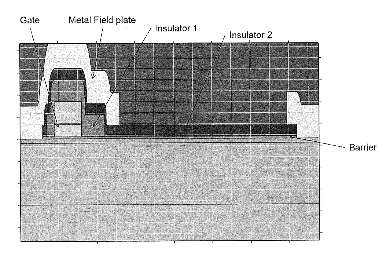
[0056]FIG. 4 illustrates a cross-sectional view of a GaN transistor formed according to the present invention. FIG. 4 depicts a more accurate picture showing the locations and relative dimensions of insulator 1 and insulator 2. Also included in FIG. 4 is a metal field plate that protects the gate region from high fields. The metal field plate is positioned above insulator 1 in its entirety, while being positioned above only a portion of insulator 2.

[0057]The various layers in the transistors shown in FIGS. 3 and 4 or other embodiments below and / or in any of the drawings may be formed using the processes described for fabricating the device in FIG. 2 in U.S. Pat. No. 8,350,294, issued to Lidow et al. For example, the buffer, channel, barrier, and gate layers may each be formed by, for example, nucleation. Once the gate metal is deposited, patterning and then etching of the gate material may be performed. The insulator 1 is deposited, then patterned, following by selective etching in ...

third embodiment

[0072]FIG. 11 illustrates a cross-sectional view of a GaN transistor formed according to the present invention. As shown in FIG. 11, an insulator offset layer is positioned between the second insulator and the barrier layer 134.

[0073]FIG. 12 is a band diagram of an insulator over a barrier layer while using an intermediary semiconductor (insulator) offset layer in the band gap according to the third embodiment of the present invention. The third embodiment is based on moving the trap-containing insulator, such as SiN, farther away from the channel by use of a semiconductor offset layer between the barrier and the second insulator. By making it a wide bandgap material for one of the layers, a higher barrier is created for the hot electrons to overcome.

[0074]FIGS. 13A-13G illustrate an exemplary process flow for fabricating the GaN transistor according to the second embodiment of the present invention,

[0075]FIG. 14 illustrates the formation of the GaN transistor according to the third...


PUM


Abstract

A gallium nitride (GaN) transistor which includes two or more insulator semiconductor interface regions (insulators). A first insulator disposed between the gate and drain (near the gate) minimizes the gate leakage and fields near the gate that cause high gate-drain charge (Qgd). A second insulator (or multiple insulators), disposed between the first insulator and the drain, minimizes electric fields at the drain contact and provides a high density of charge in the channel for low on-resistance.

Description

CROSS REFERENCE TO RELATED APPLICATIONS[0001]This application claims priority from U.S. Provisional Application No. 62 / 344,151, filed on Jun. 1, 2016, and U.S. Provisional Application No. 62 / 468,151, filed on Mar. 7, 2017, the disclosures of which are hereby incorporated herein by reference in their entireties.FIELD OF THE INVENTION[0002]The present invention relates to the field of column III nitride transistors such as gallium nitride (GaN) transistors. More particularly, the invention relates to GaN transistors with multiple insulator semiconductor interface regions.BACKGROUND OF THE INVENTION[0003]Gallium nitride (GaN) semiconductor devices are increasingly desirable for power semiconductor devices because of their ability to carry large current and support high voltages. Development of these devices has generally been aimed at high power / high frequency applications. Devices fabricated for these types of applications are based on general device structures that exhibit high elect...

Claims


Application Information

Patent Timeline
Patent Type & Authority Applications(United States)
IPC IPC(8): H01L29/778H01L29/40H01L29/20H01L29/205H01L29/66H01L29/51
CPCH01L29/7787H01L29/402H01L29/66462H01L29/513H01L29/205H01L29/2003H01L23/3171H01L29/7786H01L29/1066
Inventor BEACH, ROBERTSTRITTMATTER, ROBERTZHOU, CHUNHUAZHAO, GUANGYUANCAO, JIANJUN
Owner EFFICIENT POWER CONVERSION CORP
Why Eureka
Try Eureka