

Plasma CVD apparatus, method for forming microcrystalline semiconductor film and method for manufacturing semiconductor device
a technology of microcrystalline semiconductor and plasma cvd, which is applied in the direction of coatings, chemical vapor deposition coatings, electric discharge tubes, etc., can solve the problems of inability to form dense microcrystalline semiconductor films and inability to form dense semiconductor films, so as to reduce the number of amorphous components in a deposited microcrystalline semiconductor film
- Summary
- Abstract
- Description
- Claims
- Application Information
AI Technical Summary
Benefits of technology
Problems solved by technology
Method used
Image

Examples
embodiment 1
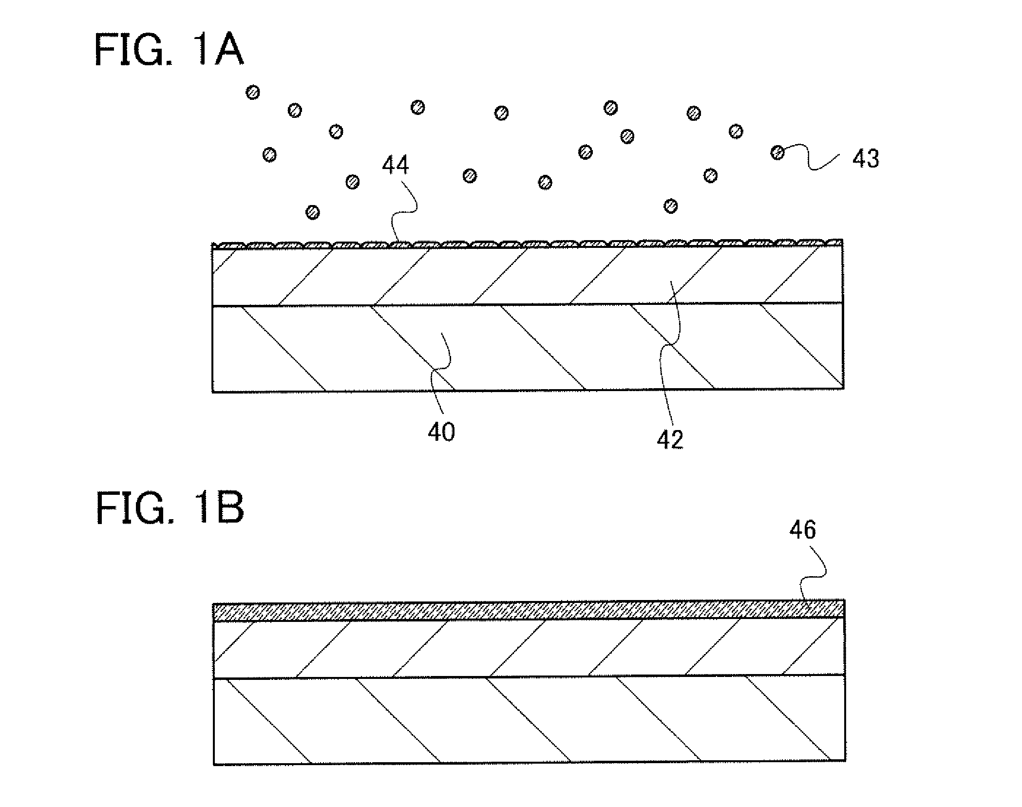
[0042]In this embodiment, a method for forming a microcrystalline semiconductor film having high crystallinity is described with reference to FIGS. 1A and 1B, FIG. 2, FIGS. 3A and 3B, FIGS. 4A and 4B, FIGS. 5A and 5B, FIGS. 6A and 6B, FIG. 7, FIGS. 8A to 8D, FIGS. 17A and 17B, FIGS. 18A and 18B, and FIGS. 19A and 19B.
[0043]As illustrated in FIG. 1A, in a method for forming a microcrystalline semiconductor film shown in this embodiment, deposition precursors 43 are formed in a gas phase, the deposition precursors 43 are deposited over a base film 42 which is formed over a substrate 40, and crystal nuclei 44 are formed. Next, as illustrated in FIG. 1B, a microcrystalline semiconductor film is formed over the crystal nuclei 44, whereby crystals are grown using the crystal nuclei 44 as nuclei so that a microcrystalline semiconductor film 46 can be formed.
[0044]The deposition precursor 43 is formed through reaction of electrons and a source gas in plasma. The pressure in a film formation...
embodiment 2
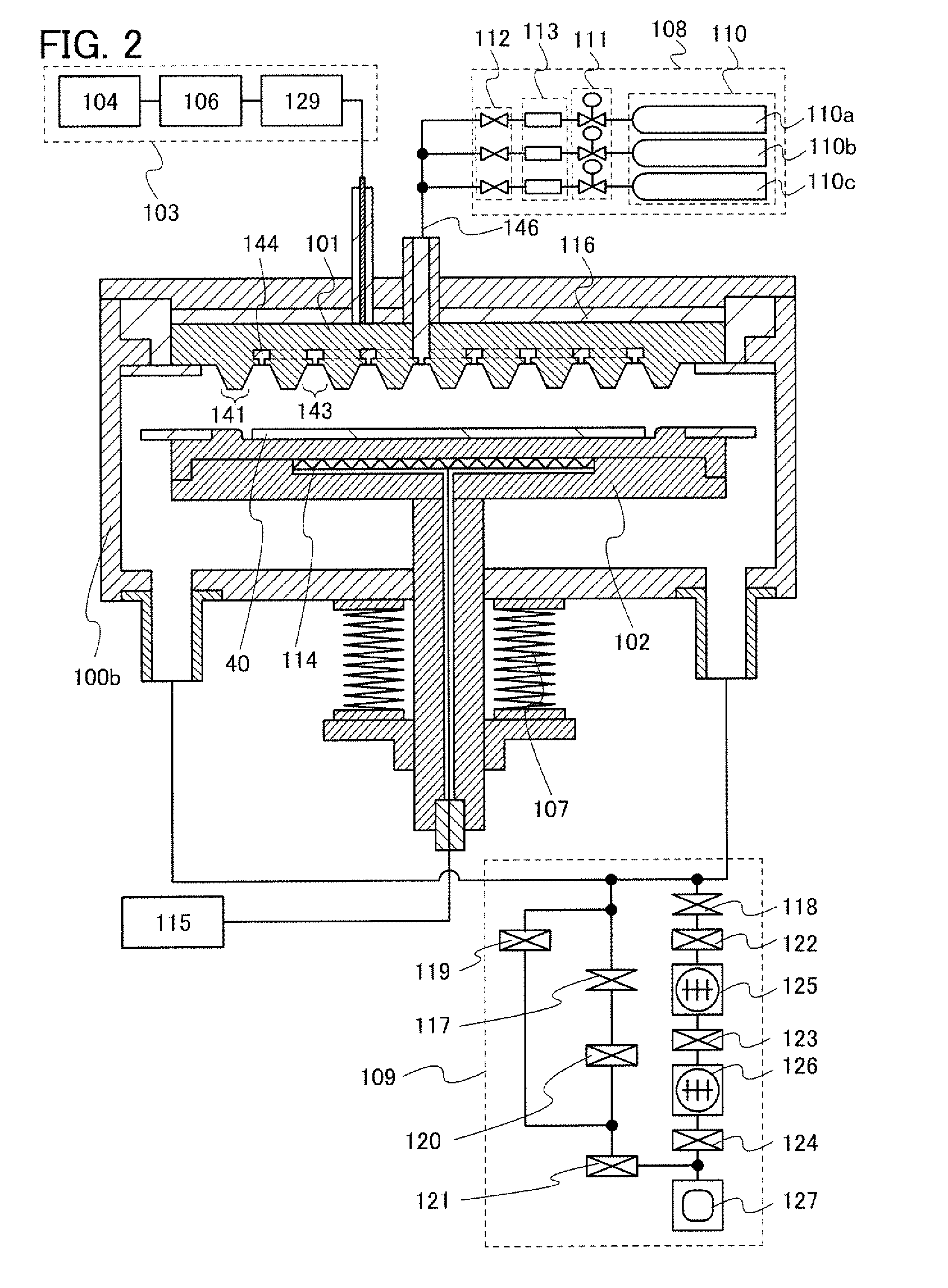
[0102]In this embodiment, one mode of the shape of the first electrode 101 is described with reference to FIGS. 9A and 9B. FIG. 9A is a plan view of the first electrode 101 seen from the second electrode 102 side. FIG. 9B is a cross-sectional view taken along A-B in FIG. 9A. Note that in FIG. 9A, regions which are projected to the second electrode side (that is, projected portions) are shown by a wide hatch pattern and regions which are depressed (that is, depressed portions) are shown by a narrow hatch pattern for clear illustration of the state of the projection and depression.
[0103]As illustrated in FIGS. 9A and 9B, gas supply ports of hollow portions 142 formed on the common plane are provided regularly, preferably at regular intervals. Further, the gas supply ports of the hollow portions 142 are provided in the projected portions 141. The plurality of depressed portions 143 are separated from one another, and the projected portions 141 form a continuous plane (common plane). He...
embodiment 3
[0105]In this embodiment, a method for forming a microcrystalline semiconductor film having much higher crystallinity than the microcrystalline semiconductor films in Embodiments 1 and 2 is described.
[0106]In this embodiment, as a source gas of the deposition precursor 43 and the microcrystalline semiconductor film 46 in FIGS. 1A and 113, a rare gas such as argon, xenon, or krypton is used in addition to hydrogen and a deposition gas containing silicon or germanium.
[0107]Electron density and the amount of hydrogen radicals in plasma are increased by using a rare gas such as argon, xenon, or krypton, as a source gas, which has low excitation energy and has metastable energy close to dissociation energy of silane and hydrogen. Further, because electron temperature is lowered, potential difference in plasma is reduced and damage to the microcrystalline semiconductor film is reduced, whereby the microcrystalline semiconductor film 46 having high crystallinity is formed. By using a rare ...
PUM
| Property | Measurement | Unit |
|---|---|---|
| Pressure | aaaaa | aaaaa |
| Pressure | aaaaa | aaaaa |
| Length | aaaaa | aaaaa |
Abstract
Description
Claims
Application Information