Laminated circuit board and its manufacturing method, and manufacturing method for module using the laminated circuit board and its manufacturing apparatus

a manufacturing method and technology of laminated circuit boards, applied in the direction of printed circuit non-printed electric component association, printed circuit electric connection formation, high frequency circuit adaptations, etc., can solve the problems of physical difficulty in manufacturing laminated circuit boards, defective insulation, and affect the connection of electronic components b>3/b>, and achieve high reliability in electric connection

Inactive Publication Date: 2005-06-02
PANASONIC CORP
View PDF2 Cites 28 Cited by
  • Summary
  • Abstract
  • Description
  • Claims
  • Application Information

AI Technical Summary

Benefits of technology

[0013] The purpose of the present invention is to provide a laminated circuit board which may ...

Problems solved by technology

However, in such a conventional laminated circuit board 670 with electronic component 3 buried therein, as the mounting density of electronic component 3 is increased, there arises the following problem.
Therefore, it is physically difficult to manufacture laminated circuit board 670.
A great stress then applied is the cause of a problem such that the connection of ele...

Method used


Image

  • Laminated circuit board and its manufacturing method, and manufacturing method for module using the laminated circuit board and its manufacturing apparatus
  • Laminated circuit board and its manufacturing method, and manufacturing method for module using the laminated circuit board and its manufacturing apparatus
  • Laminated circuit board and its manufacturing method, and manufacturing method for module using the laminated circuit board and its manufacturing apparatus

Examples


embodiment 1

Preferred Embodiment 1

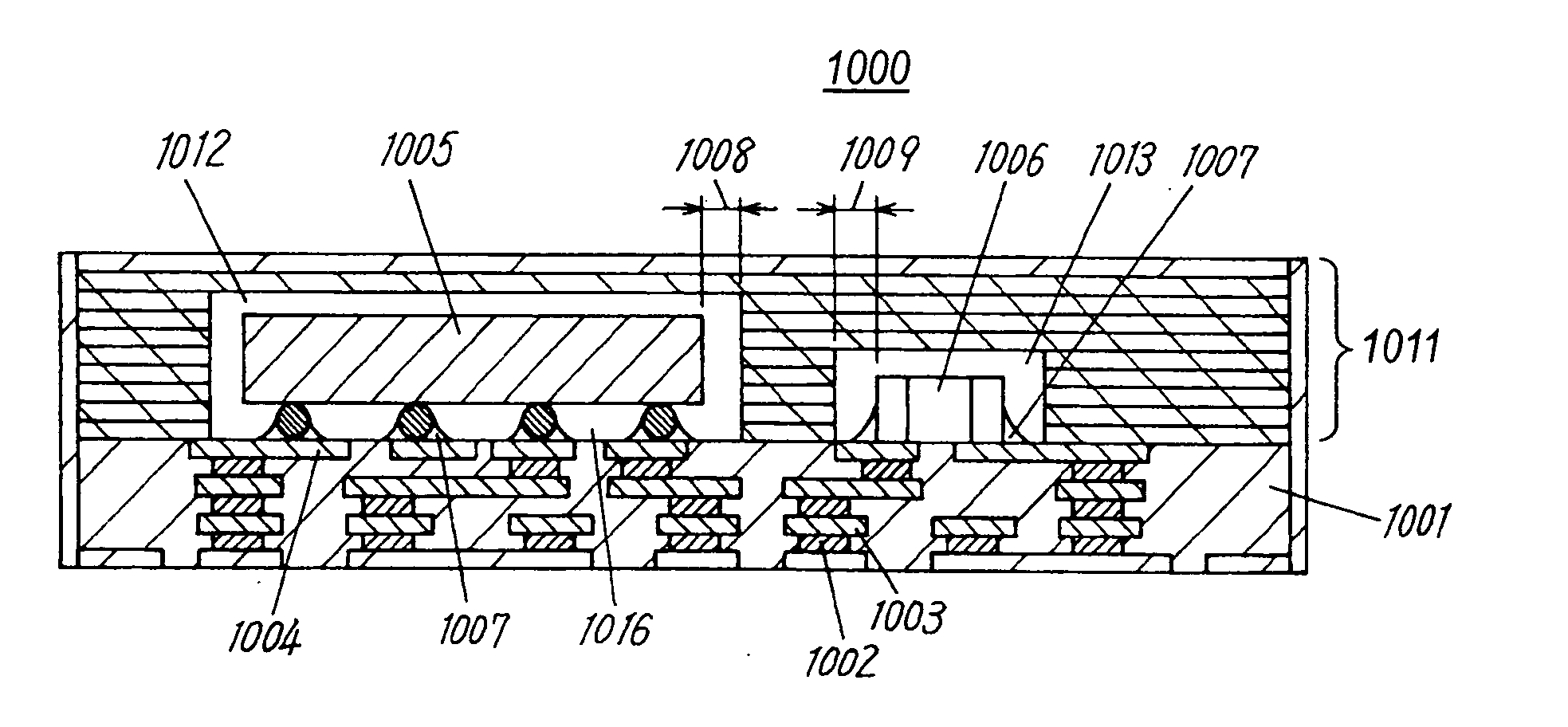
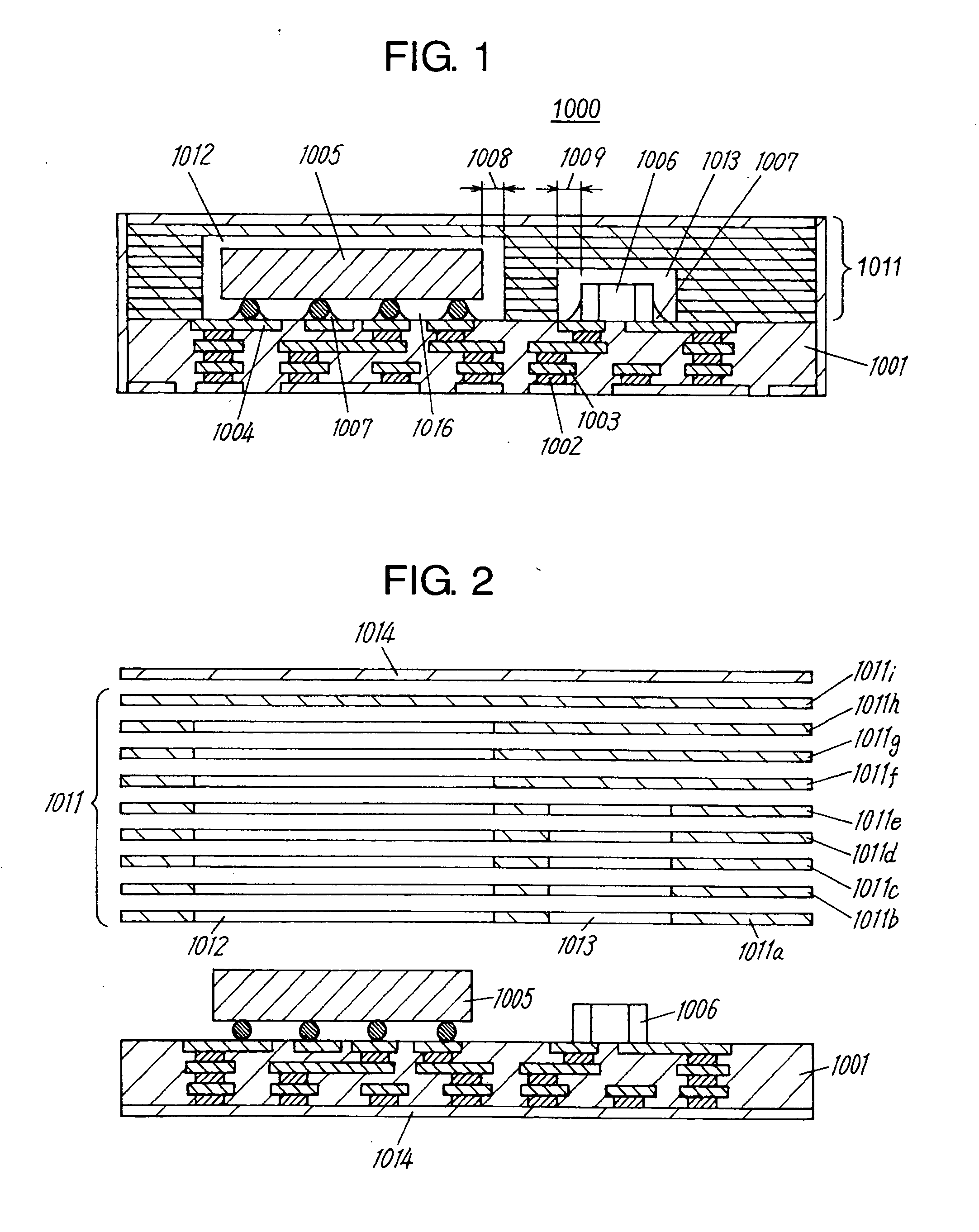
[0118]FIG. 1 is a sectional view of laminated circuit board 1000 in the preferred embodiment 1 of the present invention. In FIG. 1, thermosetting resin substrate 1001 is formed in multiple layers. And, the interior of thermosetting resin substrate 1001 is inner-via 1002, and one main surface of each layer is electrically connected to the opposite side or the other main surface. Each layer is provided with copper foil pattern 1003, thereby forming various electronic circuits. And, on one main surface of resin substrate 1001 is formed land pattern 1004. Further, electronic components such as integrated circuit 1005 and resistor 1006 for example are connected to this one main surface by solder 1007.

[0119] Lead-free solder using tin, silver or copper is used as solder 1007, which contains no substance harmful to human body and gives no bad influences to the environment. Also, a conductive bonding agent of thermosetting type can be used instead of solder 1007. When...

embodiment 2

Preferred Embodiment 2

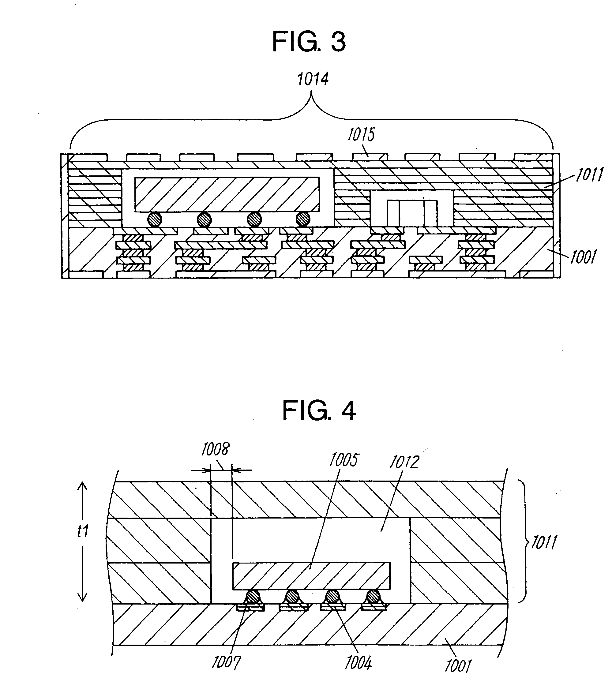
[0139]FIG. 7A is an enlarged sectional view of an essential portion in the vicinity of integrated circuit 1005 of a laminated circuit board in the preferred embodiment 2 of the present invention. In the preferred embodiment 2, holes (openings) formed in sheet 1011 will be described in detail.

[0140] Hole 1012 is disposed in sheet 1011. Also, hole 1012 is set to a size having a pace and some clearance capable of storing integrated circuit 1005 soldered to resin substrate 1001. In this condition, when thermo-compression bonding is executed under the predetermined bonding conditions, resin 1016 having heat fluidity flows out of main body 1011a of sheet 1011, then the density of porous fiber (glass fiber) forming woven or non-woven cloth increases at main body 1011a side. Also, hole 1012 is filled with resin 1016. Incidentally, the predetermined bonding conditions can be set, as described in the preferred embodiment 1, for example such that the thermo-compression b...

embodiment 3

Preferred Embodiment 3

[0144]FIG. 8 is a sectional view of a laminated circuit board in the preferred embodiment 3. Integrated circuit 1005 is connected by soldering onto one main surface of resin substrate 1001. Also, next to integrated circuit 1005 is placed inductor 1031 as an example of circuit pattern as shown in FIG. 9.

[0145] Hole 1032 is an opening disposed in sheet 1030 of sheet 1011. Hole 1032 is provided so as to cover integrated circuit 1005 and inductor 1031. That is, integrated circuit 1005 is mounted in a position eccentric to hole 1032. Since hole 1032 is formed in this way, resin 1016 is sufficiently filled even around inductor 1031.

[0146] The dielectric constant of resin 1016 is selected to be in a range of about 6.5 to 9.5. Therefore, it is larger by about 2.3 as compared with the dielectric constant of conventional porous fiber, and it is possible to reduce the size of inductor 1031.

[0147] The impedance of inductor 1031 is in reverse proportion to the square roo...


PUM


Abstract

A laminated circuit board with electronic components buried therein comprises a substrate on which a land disposed on one main surface thereof is connected and fixed by solder to an integrated circuit (or the like). A sheet is laminated on the upper surface of the substrate. A filling portion by fluid resin is formed by clearance at the outer periphery of the integrated circuit (or the like). The sheet maintains its shape by woven or non-woven cloth having a hole in which the integrated circuit (or the like) is buried. The woven or non-woven cloth is impregnated with resin having heat fluidity and is thermally compressed. Thus, the electrical and mechanical connections between the laminated circuit board and electronic component can be enhanced in reliability.

Description

TECHNICAL FIELD [0001] The present invention relates to a laminated circuit board with electronic components buried therein and its manufacturing method, and a manufacturing method for a module using the laminated circuit board and its manufacturing apparatus. BACKGROUND ART [0002] A laminated circuit board with electronic components buried therein will be described with reference to FIG. 67. Laminated circuit board 670 with electronic components buried therein is such that substrates 2a to 2e formed from thermoplastic resin are laminated on one main surface of substrate 1 formed of a metallic base member. [0003] The words “one main surface” and “the other main surface” used in the following description respectively stand for one surface in the direction of thickness and the opposite side surface in those being relatively less in thickness than the sizes of length and width such as resin boards or various sheets. Accordingly, the word “one main surface” does not mean only a “surface...

Claims


Application Information

Patent Timeline
IPC IPC(8): H01L21/04H01L21/50H01L25/00H01L25/16H05K1/02H05K1/16H05K1/18H05K3/00H05K3/34H05K3/40H05K3/46
CPCH05K1/186Y10T156/1052H05K3/3405H05K3/403H05K3/4069H05K3/4614H05K3/4652H05K2201/0187H05K2201/086H05K2201/09181H05K2201/10371H05K2203/0169H05K2203/0191H05K2203/0568H05K2203/063H01L21/50H01L24/97H01L25/165H01L2224/16225H01L2924/01009H01L2924/01013H01L2924/01015H01L2924/01027H01L2924/01029H01L2924/0103H01L2924/01033H01L2924/01047H01L2924/01075H01L2924/01078H01L2924/01082H01L2924/14H01L2924/15153H01L2924/1517H01L2924/16152H01L2924/16195H01L2924/19041H01L2924/19042H01L2924/19043H01L2924/19105H01L2924/30105H01L2924/30107H01L2924/3011H01L2924/3025H05K1/024H05K1/165H01L2924/01005H01L2924/01006H01L2924/12041Y10T156/1057Y10T156/12H05K3/0052H01L2924/12034H01L2924/12042H01L2924/00
Inventor KIMURA, JUNICHINISHII, TOSHIHIROOCHI, AKIOHARADA, SHINJI
Owner PANASONIC CORP
Why Eureka
Try Eureka