Interface structure

a technology of interface structure and interface plate, which is applied in the direction of fixed connections, coupling device connections, instruments, etc., can solve the problems of poor electrical connection between the probe pin and the electrode pad, high electrical resistance, and inability to easily remove the socket from the board, so as to reduce the electrical resistance, shorten the current path through the plating, and reduce the effect of electrical resistan

Active Publication Date: 2020-07-14
LTI HLDG INC
View PDF65 Cites 0 Cited by
  • Summary
  • Abstract
  • Description
  • Claims
  • Application Information

AI Technical Summary

Benefits of technology

[0008]The present disclosure solves the above problems and intends to provide an inexpensive interface structure that enables highly reliable electrical connection.
[0012]According to the present disclosure, the inner wall of the through hole of the main portion is plated and the coil spring for contacts is received in the through hole, so that the interface structure may be inexpensive compared with the structure with conventional probe pins and may shorten the current path through the plating of the inner wall of the through hole, thereby reducing the electrical resistance.

Problems solved by technology

In such mounting, since the terminals of the socket and the circuit board are directly connected each other by the solder, the socket cannot be easily removed from the board.
If there are foreign materials attached on the electrode pad, or the surface of the electrode pad is oxidized, poor electrical connection between the probe pin and the electrode pad or high electrical resistance are caused.
As the result, the reliable good electrical connection between the semiconductor device and the circuit board cannot be achieved, and furthermore, such semiconductor device may be judged as defective in burn-in test process, even if it is not defective.
Furthermore, the conventional adaptor for socket may be relatively expensive because probe pins require complex working processes for combining the coil spring and the probe pin.

Method used


Image

  • Interface structure
  • Interface structure
  • Interface structure

Examples


Embodiment Construction

[0027]The subject technology overcomes many of the prior art problems of socket adapators. The advantages, and other features of the technology disclosed herein, will become more readily apparent to those having ordinary skill in the art from the following detailed description of certain preferred embodiments taken in conjunction with the drawings which set forth representative embodiments of the present invention and wherein like reference numerals identify similar structural elements. References such as up, down, upper, lower, right and left are generally with respect to the figures and not meant in a limiting sense.

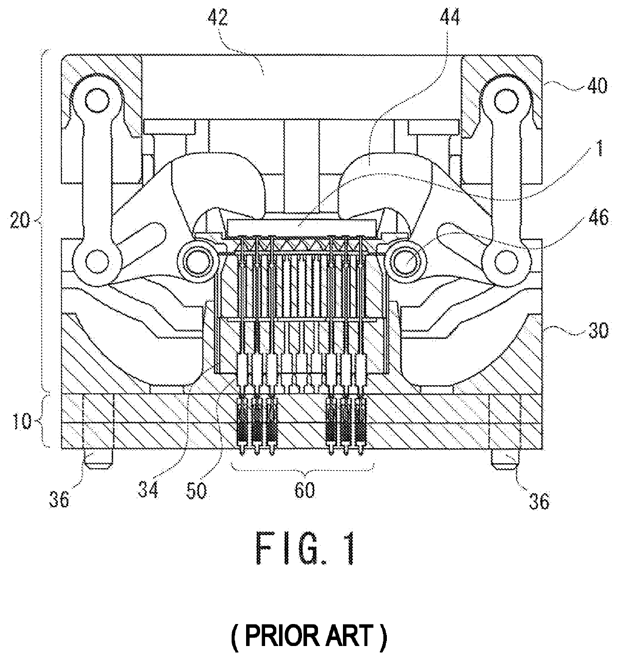
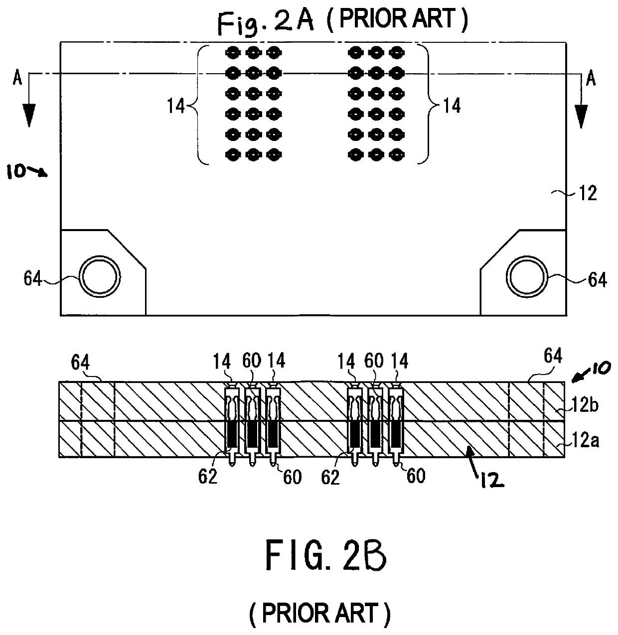
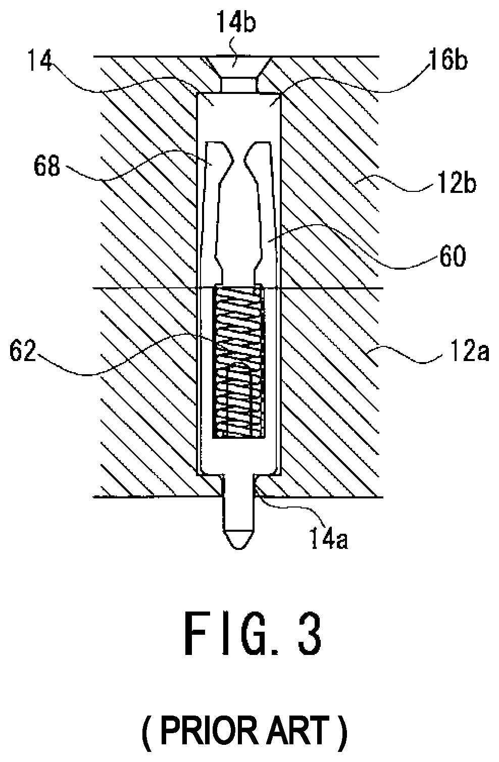
[0028]Now embodiments according to the present disclosure will be described in detail with reference to the accompanying drawings. In a preferred embodiment, the interface structure according to the present disclosure is carried out as an adaptor for socket. It should be noted that the drawings emphasize each portion for clarity and are not necessarily drawn to scale w...


PUM

PropertyMeasurementUnit
angleaaaaaaaaaa
interface structureaaaaaaaaaa
external diameteraaaaaaaaaa

Abstract

An interface structure connecting an electronic component to a circuit board. The interface structure includes a base defining an elongated through hole with a central axis and a coil spring retained in the elongated through hole. The coil spring has a proximal portion and a distal portion extending from the elongated through hole in an uncompressed condition and being offset at an angle with respect to the central axis. As the coil spring is compressed, the coil spring creates a force having a component substantially perpendicular to the central axis.

Description

CROSS-REFERENCE TO RELATED APPLICATION[0001]This application claims the benefit of Japanese Patent Application No. 2015-242793 filed Dec. 14, 2015, which is incorporated herein by reference.BACKGROUND OF THE INVENTION[0002]The present disclosure relates to an interface structure using spring contacts, particularly to the interface structure for detachably connecting an electronic component such as an IC socket to a board.[0003]IC sockets have been widely used as an interface for electrically connecting a semiconductor device to a print board. An IC socket loading a surface-mount type semiconductor device such as BGA (Ball Grid Array), CSP (Chip Sized Package) or LGA (Land Grid Array) includes a base member on which the bottom surface of the semiconductor device is loaded, and a cover member that presses the loaded semiconductor device to the base member so as to allow solder balls at the bottom of the semiconductor device to contact with probe pins [See, for example, Japanese Patent...

Claims


Application Information

Patent Timeline
Patent Type & Authority Patents(United States)
IPC IPC(8): H01R12/70H01R13/24H05K7/10H01R12/71H01R13/11H01R13/631H05K3/32H01R43/20H01R24/58G01R1/04G01R3/00
CPCH01R13/631H01R43/205H05K3/32H01R12/716G01R1/0466H01R43/20H01R13/2421H01R13/111H01R12/7076H05K7/10H01R24/58Y10T29/49218H01R12/714G01R1/0458Y10T29/49151Y10T29/49208G01R3/00H01R12/57H01R13/035H01R13/187G01R31/2889G01R31/2863G01R1/0408G01R1/073
Inventor TAKAHASHI, HIDEYUKI
Owner LTI HLDG INC
Why Eureka
Try Eureka