Mounting structure, electro-optical apparatus, and electronic apparatus
a technology of mounting structure and electrooptical apparatus, applied in the direction of electrical apparatus construction details, circuit inspection/indentification, printed circuit aspects, etc., can solve the problems of reducing the size of the element substrate and the fpc, and the difficulty of properly positioning the element substrate, etc., to achieve high reliability in electrical connection
- Summary
- Abstract
- Description
- Claims
- Application Information
AI Technical Summary
Benefits of technology
Problems solved by technology
Method used
Image
Examples
first embodiment
Electro-Optical Apparatus
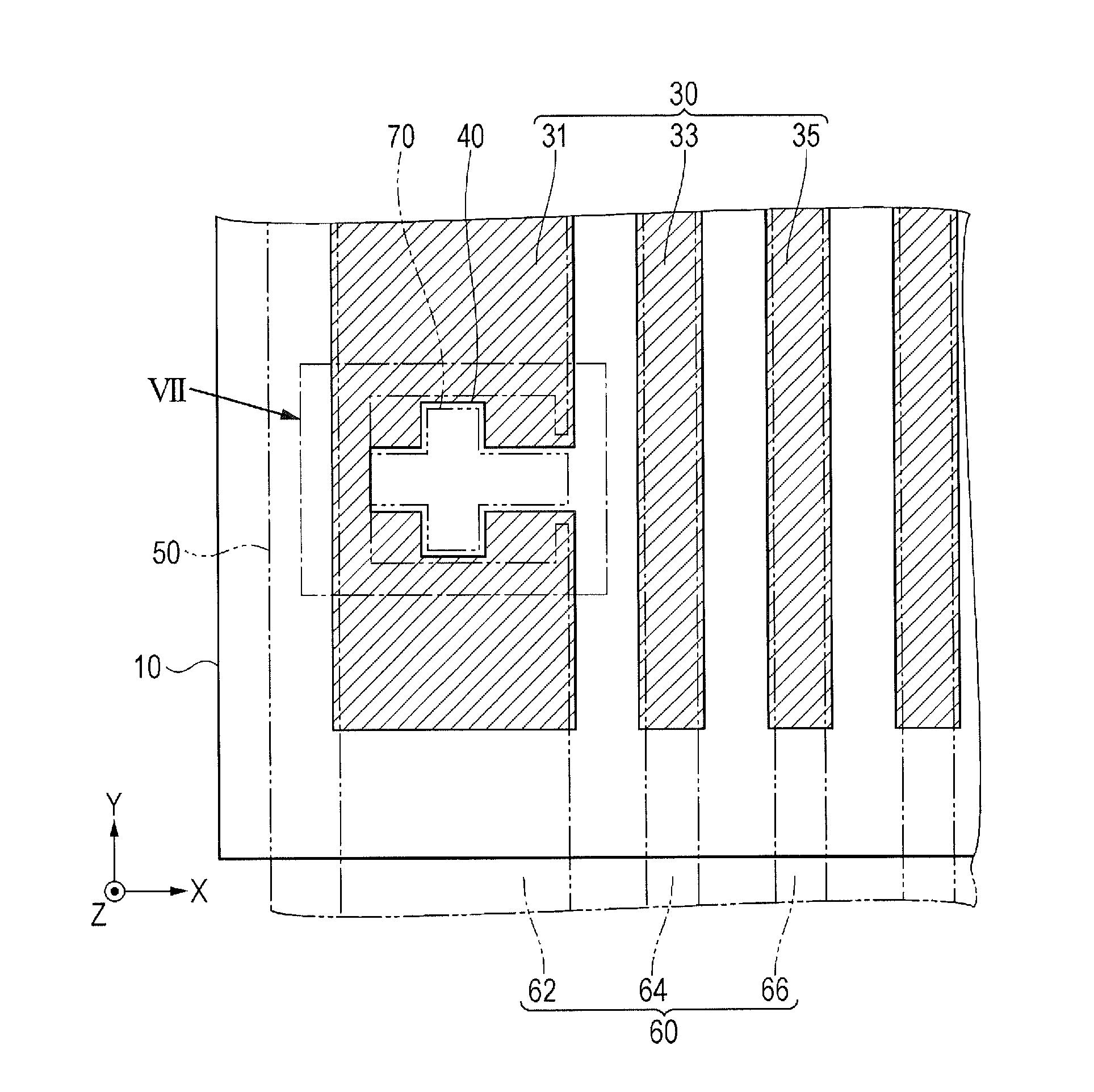
[0063]Referring first to FIG. 1, an organic EL apparatus according to a first embodiment, exemplifying an electro-optical apparatus to which the mounting structure in the present invention is applied, will be described.
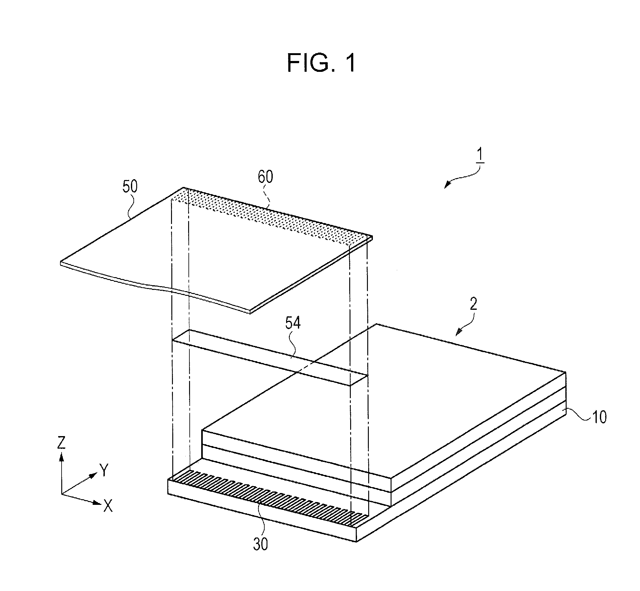
[0064]FIG. 1 is an exploded perspective view showing a configuration of the organic EL apparatus according to a first embodiment, exemplifying the electro-optical apparatus in the present invention.
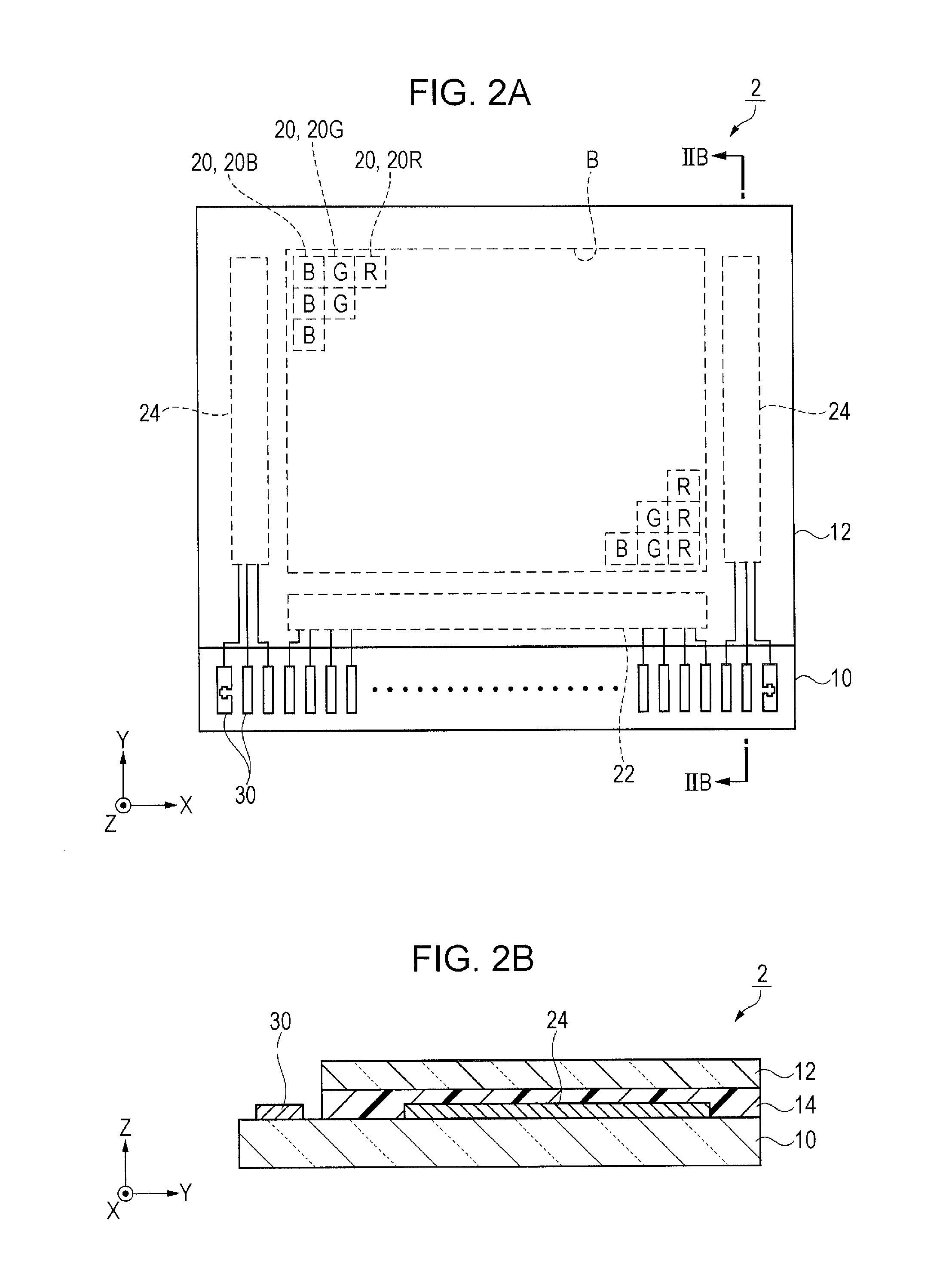
[0065]The organic EL apparatus 1 according to the first embodiment includes an organic EL panel 2 including an element substrate 10 having an organic EL element provided thereon and an FPC 50. The element substrate 10 corresponds to the first substrate, the organic EL element corresponds to the electro-optical element, and the FPC 50 corresponds to the second substrate in the present invention.
[0066]A plurality of terminals 30 are provided on the element substrate 10, and a plurality of terminal 60 are provided on the surface of the FPC 50 opposing ...
second embodiment
[0099]Referring to FIGS. 8A to 10, configurations of a first alignment mark and a second alignment mark according to a second embodiment will be described hereunder.
[0100]FIG. 8A is a plan view of an element substrate 10a and FIG. 8B is a plan view (see-through view) of an FPC 50a, for explaining the alignment marks according to the second embodiment. FIG. 8B illustrates terminals 60a and the second alignment mark 70a on the FPC 50a seen through from the side of the FPC 50a, for facilitating the understanding of the positional relationship with respect to terminals 30a and the first alignment mark 40a on the element substrate 10z shown in FIG. 8A.
[0101]The first alignment mark 40a and the second alignment mark 70a according to the second embodiment are different in shape from the first alignment mark 40 and the second alignment mark 70 according to the first embodiment. Therefore, the same constituents as those of the first embodiment are given the same numeral with “a”, and the des...
third embodiment
[0107]Referring to FIGS. 11A and 11B, configurations of a first alignment mark and a second alignment mark according to a third embodiment will be described hereunder.
[0108]FIG. 11A is a plan view of an element substrate 10b and FIG. 11B is a plan view (see-through view) of an FPC 50b, for explaining the alignment marks according to the third embodiment.
[0109]The first alignment mark 40b and the second alignment mark 70b according to the third embodiment are different in shape from the first alignment mark 40 and the second alignment mark 70 according to the first embodiment. Therefore, the same constituents as those of the first embodiment are given the same numeral with “b”, and the description thereof will not be repeated.
[0110]As shown in FIGS. 11A and 11B, the first alignment mark 40b is formed so as to span over the first terminal 31b, which is wider in the X-axis direction than other terminals 30b provided on the element substrate 10b of the organic EL panel 2b, and a third t...
PUM
 Abstract
Description
Claims
Application Information


