Method for forming wiring pattern, wiring pattern, and electronic apparatus

a technology of electronic equipment and wiring patterns, applied in the direction of liquid/solution decomposition chemical coating, instrumentation, semiconductor/solid-state device details, etc., can solve the problems of high manufacturing cost, complicated process, and huge lithography facilities, and achieve high reliability of electrical connection, low manufacturing cost, and simplified droplet discharge process

Active Publication Date: 2009-12-08
SEIKO EPSON CORP
View PDF13 Cites 0 Cited by
  • Summary
  • Abstract
  • Description
  • Claims
  • Application Information

AI Technical Summary

Benefits of technology

[0009]An advantage of the invention is to provide a method for forming a wiring pattern that is suitable for forming a conductive post. Another advantage of the invention is to provide a wiring pattern and an electronic apparatus that realize a low manufacturing cost and a highly reliable electrical connection.
[0010]Therefore, a first aspect of the invention is to provide a method for forming a wiring pattern in which a plurality of electrical wirings deposited onto a substrate is conductively connected with each other through a plurality of conductive posts. The method includes relatively moving a discharge head having a plurality of nozzles and the substrate in a predetermined direction while discharging droplets from predetermined nozzles among the plural nozzles to form the plural conductive posts. Here, in the orthogonal direction of the above-referenced predetermined direction, the interval among the plural nozzles “a” and the interval among the plural conductive posts “b” must satisfy an equation “b=m×a” (“m” may be any positive integer).
[0011]According to the method, due to the requirement that the interval among the plural conductive posts is equal to integral multiples of the interval among the plural nozzles, a droplet discharge process can be simplified. Specifically, in the relative movement of the discharge head and the substrate, the droplets can be placed in a single relative movement on each of the positions on which the plural conductive posts to be formed, because, due to the requirement, once a conductive post forming position is placed on a moving axis of one of the plural nozzles, other conductive post forming positions are also placed on moving axes of the other nozzles. Therefore, the relative movement can be done more efficiently, simplifying a droplet discharge process.
[0012]In the method for forming a wiring pattern, the discharging and the preliminary drying of droplets are repeated so that the plural conductive posts may be deposited. Multilayered posts are formed by the repetition of the discharging and the preliminary drying of droplets. Then, the laminated structure ensures an appropriate height for a post to be formed. Further, the method suppresses an increase of processing time involved with the repeating of droplets discharging, because there is little waste in the relative movement of the discharge head and the substrate as described above.
[0013]Here, the method includes forming of liquid lines to form the plural electrical wirings, the plural conductive posts being deposited on the liquid lines. By forming the posts on the liquid lines, both can be easily coalesced on the interface. Then, by simultaneously baking the coalesced liquid lines and posts, the electrical wirings and the conductive posts can be integrally formed. As a result, the occurrence of cracks on the interface between the electrical wirings and the conductive posts can be prevented, making it possible to form a wiring pattern that has a highly reliable conductive connection.
[0014]The method of forming a wiring pattern also includes setting up on the substrate a plurality of unit areas that is subdivided in a lattice pattern for locating a droplet discharge position. Here, it is preferable that the unit areas are set up so that, in the orthogonal direction of the above-referenced predetermined direction, the interval among the plural nozzles “a” and the width of the unit area “c” satisfy an equation “c=a / n” (“n” may be any positive integer). Thus, the pattern design can be simplified.

Problems solved by technology

However, lithography requires huge facilities, such as a vacuum system, and complicated processes.
Besides, the manufacturing cost is high because the yield rate is only a few percent and the bulk of material must be thrown out.
Further, there is a limit to the refining of a wiring pattern.
However, discharging plenty of droplets at a time is not sufficient to achieve a needed height for a post.
Rather, there is a possibility that it generates a post that is too large in diameter, causing a short circuit between adjacent electrical wirings or between adjacent conductive posts.

Method used


Image

  • Method for forming wiring pattern, wiring pattern, and electronic apparatus
  • Method for forming wiring pattern, wiring pattern, and electronic apparatus
  • Method for forming wiring pattern, wiring pattern, and electronic apparatus

Examples


Embodiment Construction

[0028]Embodiments of the invention will now be described with reference to the drawings. In the drawings to be referred below, scale sizes of the components are accordingly changed so that the components can be drawn in recognizable sizes.

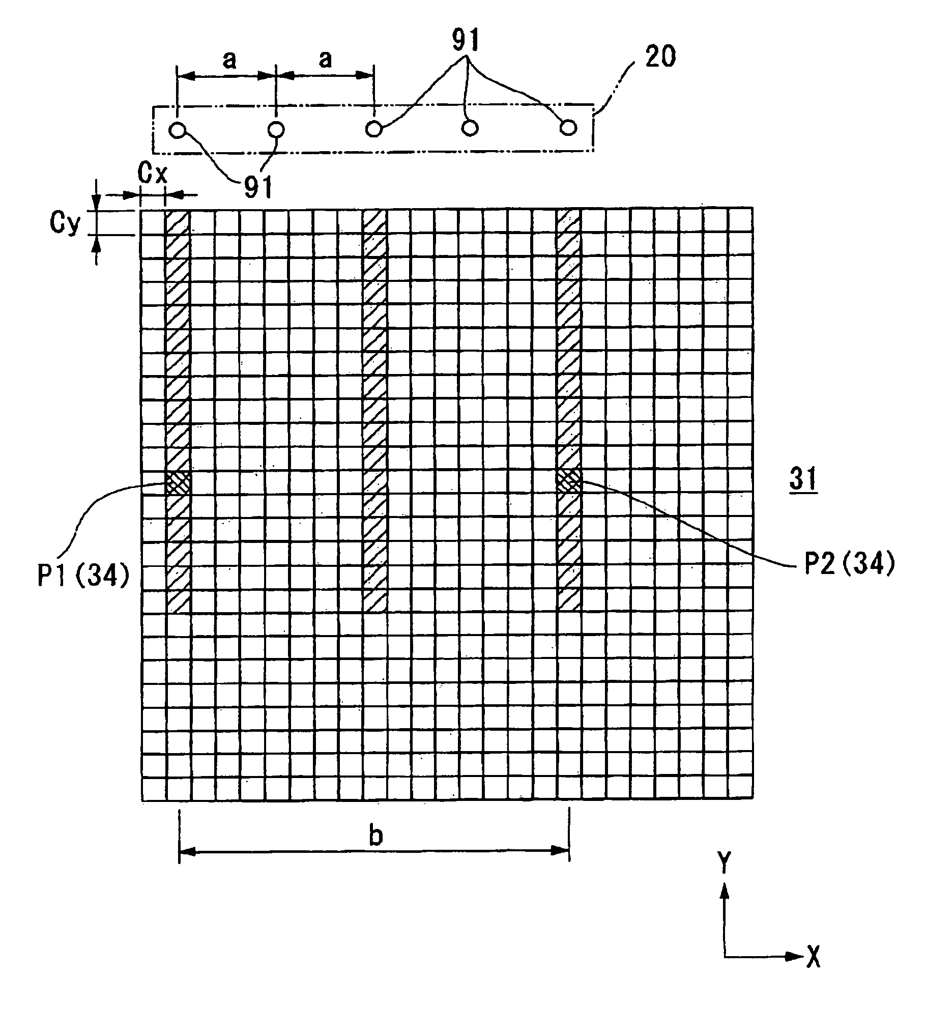
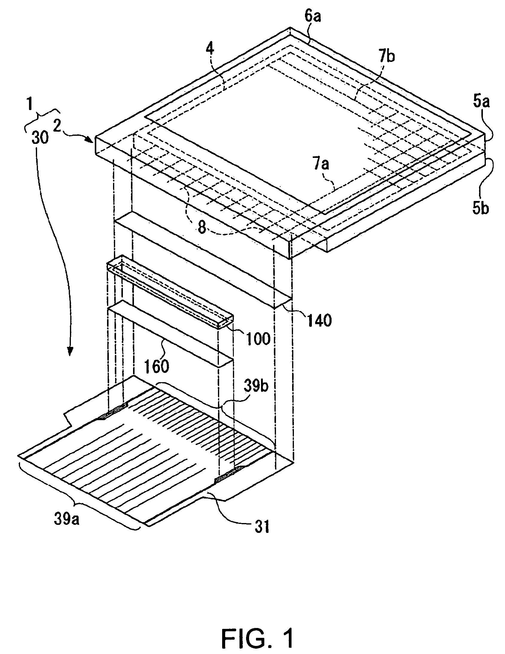
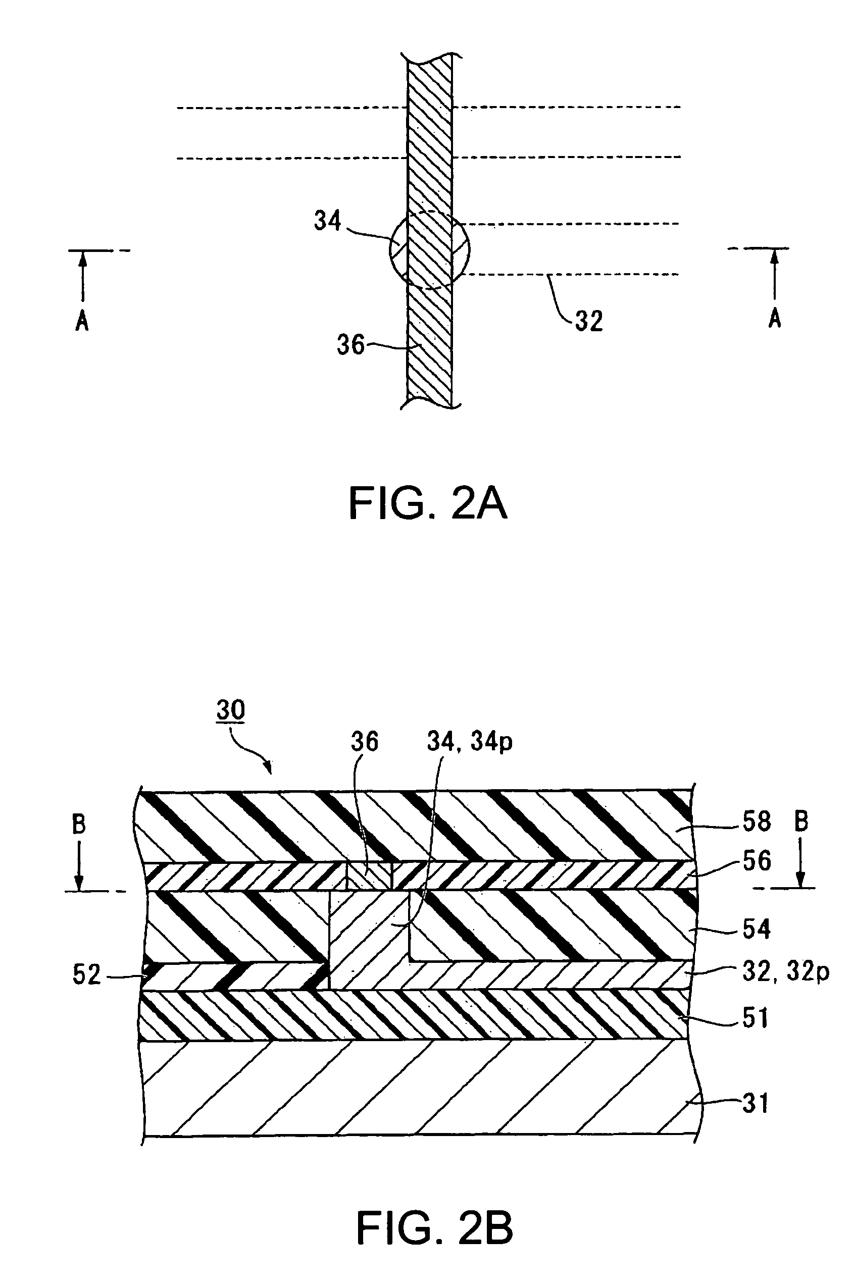
[0029]FIG. 1 is an exploded oblique diagram of a liquid crystal module with a COF (Chip On Film) structure. In the present embodiment, a method for forming a wiring pattern on a Flexible Printed Circuit 30 (hereinafter, simply referred to as an “FPC”) will be described as an example. FPC 30 includes a flexible film substrate 31, on the surface of which electrical wiring patterns 39a and 39b are formed. As is described later in detail, in the liquid crystal module 1 shown in FIG. 1, FPC 30 is connected to an edge of a liquid crystal panel 2, and a liquid crystal driving IC 100 is installed on the surface of FPC 30. Then, a driving signal is output to the liquid crystal panel 2 from the liquid crystal driving IC 100 via FPC 30 to display images on th...


PUM

PropertyMeasurementUnit
heightaaaaaaaaaa
heightaaaaaaaaaa
wavelengthaaaaaaaaaa

Abstract

A method for forming a wiring pattern in which a plurality of electrical wirings deposited onto a substrate is conductively connected with each other through a plurality of conductive posts, the method including relatively moving a discharge head having a plurality of nozzles and a substrate in a predetermined direction while discharging droplets from predetermined nozzles among the plural nozzles to form the plural conductive posts, wherein, in the orthogonal direction of the above-referenced predetermined direction, the interval among the plural nozzles “a” and the interval among the plural conductive posts “b” satisfy an equation “b=m×a” (“m” may be any positive integer).

Description

[0001]This application claims the benefit of Japanese Patent Application No. 2004-282224, filed Sep. 28, 2004. The entire disclosure of the prior application is hereby incorporated by reference herein in its entirety.BACKGROUND OF THE INVENTION[0002]1. Technical Field[0003]The present invention relates to a method for forming a wiring pattern, a wiring pattern, and an electronic apparatus.[0004]2. Related Art[0005]A wiring pattern composing an electronic apparatus is formed by using, for example, lithography. However, lithography requires huge facilities, such as a vacuum system, and complicated processes. Besides, the manufacturing cost is high because the yield rate is only a few percent and the bulk of material must be thrown out. Further, there is a limit to the refining of a wiring pattern.[0006]Therefore, as an alternative process to lithography, a method for discharging a droplet containing a functional material onto a substrate to draw and form a wiring pattern directly onto...

Claims


Application Information

Patent Timeline
Patent Type & Authority Patents(United States)
IPC IPC(8): B05D5/12
CPCH05K3/4647H05K3/125H05K3/4069H05K2203/1476H05K3/4664H05K2203/013G02F1/1343G02F1/136G02F1/1345
Inventor SAKURADA, KAZUAKIUEHARA, NOBORUSHINTATE, TSUYOSHI
Owner SEIKO EPSON CORP
Why Eureka
Try Eureka